Surface tunneling miniature electron source, array thereof and implementation method of array

An implementation method and electron source technology, applied in the field of electronic science and technology, can solve the problems of difficult large-scale array integration and low emission efficiency, and achieve the effects of high electron emission efficiency, convenient processing, and easy large-scale array integration

Active Publication Date: 2017-10-13
PEKING UNIV
View PDF9 Cites 15 Cited by
  • Summary
  • Abstract
  • Description
  • Claims
  • Application Information

AI Technical Summary

Problems solved by technology

[0005] In view of this, one of the objectives of the present invention is to overcome the technical problems of low emission efficiency and difficulty in large-scale array integration existing in existing tunneling electron sources, and provide a new type of tunneling electron source

Method used


Image

  • Surface tunneling miniature electron source, array thereof and implementation method of array
  • Surface tunneling miniature electron source, array thereof and implementation method of array
  • Surface tunneling miniature electron source, array thereof and implementation method of array

Examples


Embodiment 1

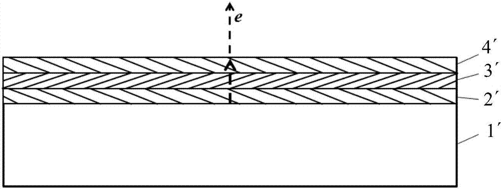
[0052] In this embodiment, the materials of the conductive region and the insulating region are embedded in the insulating substrate, and the upper surface thereof is flush with the surface of the insulating substrate.

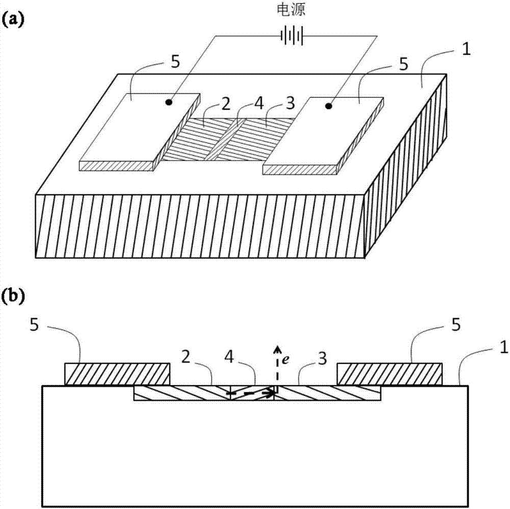
[0053] Such as figure 2 As shown, the surface tunneling miniature electron source constructed in this embodiment includes: an insulating substrate 1, conductive regions 2 and 3, an insulating region 4, and a pair of electrodes 5 for driving its electron emission.

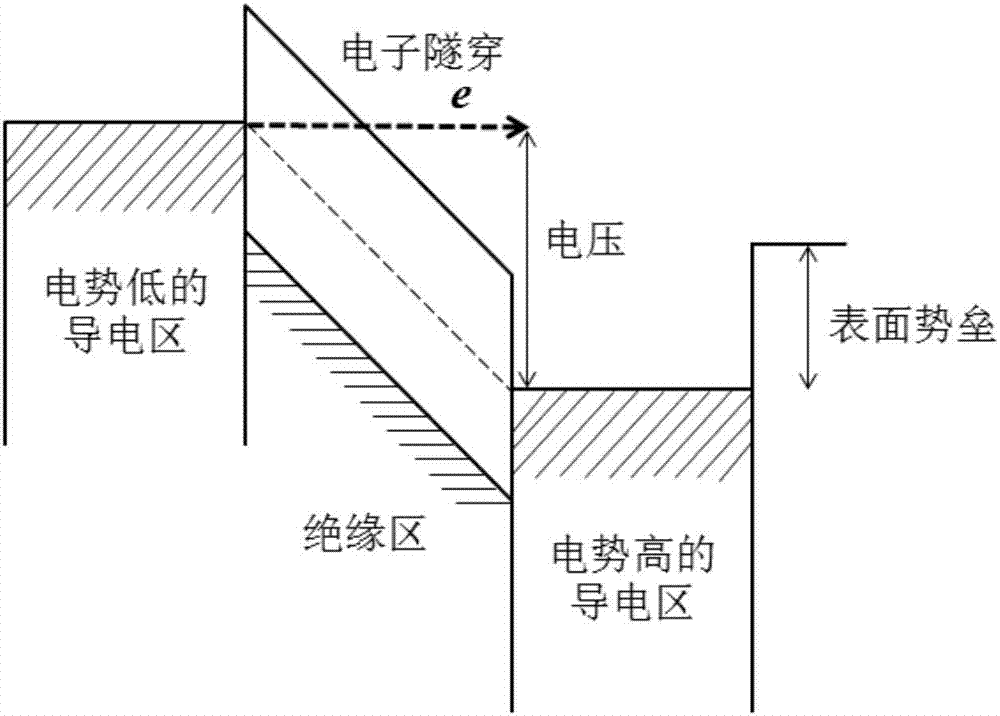
[0054] When a voltage is applied to the electrode pair 5, and the potential of the right electrode is high, electrons will tunnel from the conductive region 2 through the insulating region 4 and enter the conductive region 3, and finally vertically from the conductive region 3 close to the insulating region emitted from the surface of the substrate into vacuum.

[0055] Such as Figure 4 As shown, the surface tunneling miniature electron source array constructed in this embodiment includes: 2×5 ...

Embodiment 2

[0057] In this embodiment, the conductive region and the insulating region of the tunneling electron source are obtained by resistively switching the resistive material film to form conductive filaments, and further breaking the conductive filaments.

[0058] Such as Figure 5 As shown, the surface tunneling miniature electron source constructed in this embodiment includes: a supporting substrate 1, a resistive material film 6 covering the surface of the substrate, a pair of electrodes 5, and conductive regions 2 and 3 formed by breaking conductive filaments , Insulation area 4.

[0059] When a voltage is applied to the electrode pair 5, and the potential of the right electrode is high, electrons will tunnel from the conductive region 2 through the insulating region 4 and enter the conductive region 3, and finally vertically from the conductive region 3 close to the insulating region emitted from the surface of the substrate into vacuum.

[0060] In this embodiment, the surf...

Embodiment 3

[0065] In this embodiment, the materials of the conductive region and the insulating region are located above the surface of the insulating substrate, and their lower surfaces are flush with the surface of the insulating substrate.

[0066] Such as Figure 6 As shown, the surface tunneling miniature electron source constructed in this embodiment includes: an insulating substrate 1, conductive regions 2 and 3, an insulating region 4, and a pair of electrodes 5 for driving its electron emission.

[0067] When a voltage is applied to the electrode pair 5, and the potential of the right electrode is high, electrons will tunnel from the conductive region 2 through the insulating region 4 and enter the conductive region 3, and finally vertically from the conductive region 3 close to the insulating region emitted from the surface of the substrate into vacuum.

[0068] In this embodiment, the surface tunneling miniature electron source is realized by the following steps:

[0069] (1...


PUM


Abstract

The invention discloses a surface tunneling miniature electron source, an array thereof and an implementation method of the array. The surface tunneling miniature electron source is of a planar multi-region structure and comprises an insulation substrate, wherein two conductive regions and an insulation region are arranged on a surface of the insulation substrate, the insulation region is arranged between the two conductive regions and are connected with the two conductive regions, and the minimum distance between the two conductive regions, namely the minimum width of the insulation region is smaller than or equal to 100 nanometers. Compared with an existing tunneling electron source having a perpendicular multi-layer structure, the electron source and the array thereof have the advantages of high electron emission efficiency, simple structure, easiness in array integration on a large scale and the like, are convenient to process and can be widely applied to various electronic devices relating to the electron source, such as an X-ray tube, a microwave tube and a flat-panel display.

Description

technical field [0001] The invention belongs to the field of electronic science and technology, and in particular relates to a surface tunneling miniature electron source and its array and realization method. Background technique [0002] The electron source is considered to be the heart of vacuum electronic devices (such as X-ray tubes, high-power microwave tubes, cathode ray tubes, etc.), providing the latter with the free electron beams necessary for their work, and therefore is an essential key to vacuum electronic devices element. At present, almost all practical vacuum electronic devices use thermal emission electron sources. Since the thermal emission electron source heats the electron emitter to a high temperature (generally greater than 1000K) so that the electrons inside the emitter obtain enough kinetic energy to be emitted across the surface barrier, it has the advantages of high operating temperature, large power consumption, and preheating. Disadvantages such...

Claims


Application Information

Patent Timeline
Patent Type & Authority Applications(China)
IPC IPC(8): H01J37/073H01J9/18
CPCH01J9/18H01J37/073H01J3/022H01J9/025H01J9/027H01J23/04H01J29/028H01J35/065H01J2237/06341H01J1/304H01J1/312H01J1/316H01J2201/30449H01J2201/30461
Inventor 魏贤龙吴功涛
Owner PEKING UNIV
Why Eureka
Try Eureka