Unlock instant, AI-driven research and patent intelligence for your innovation.
Method for evaluating crystal electron density distribution model and application thereof
What is Al technical title?
Al technical title is built by PatSnap Al team. It summarizes the technical point description of the patent document.
A technology of electron density and distribution model, which is applied in the material analysis using radiation diffraction, etc., can solve the problems that the diffraction data with atomic resolution cannot be obtained, and the resolution is inferior to 0.2 nanometers.
Active Publication Date: 2017-10-20
THE NAT CENT FOR NANOSCI & TECH NCNST OF CHINA
View PDF5 Cites 1 Cited by
Summary
Abstract
Description
Claims
Application Information
AI Technical Summary
This helps you quickly interpret patents by identifying the three key elements:
Problems solved by technology
Method used
Benefits of technology
Problems solved by technology
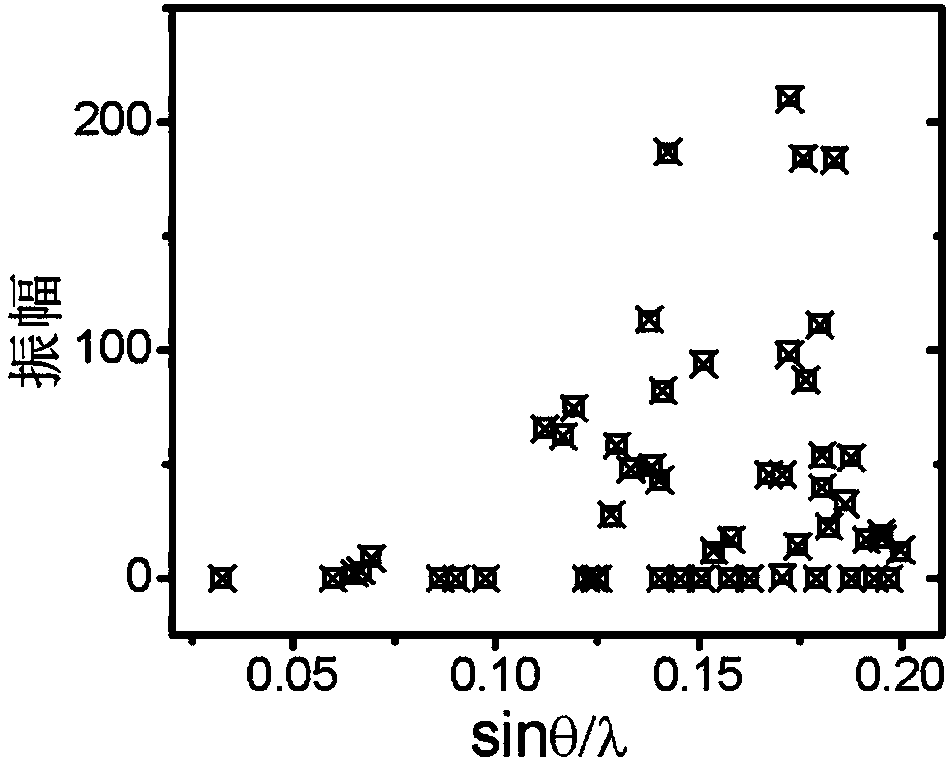
[0011] In X-raydiffraction, it is often impossible to obtain diffraction data with atomic resolution. For example, the resolution of diffraction data of macromolecular crystals such as proteins is often inferior to 0.2 nanometers.
Method used
Image
Click on the blue label to locate the original text in one second.
Reading with bidirectional positioning of images and text.
Examples
Embodiment 1
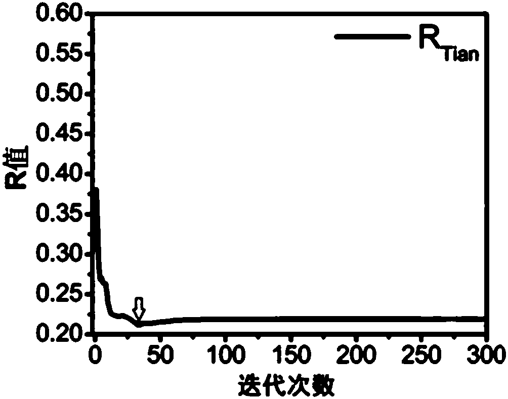
[0147] This embodiment is used to illustrate the electron density distribution model evaluation method provided by the present invention and its application in crystal structure analysis.
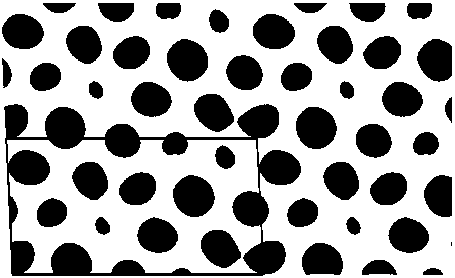
[0148] Diffractiondata source: Since the correct electron density distribution model corresponding to the diffraction data obtained from actual crystal measurement cannot be accurately known, there is a lack of strict reference standards when evaluating the quality of the electron density distribution model obtained in crystal structure analysis. To overcome this difficulty, simulated diffraction data are used in this example, and the simulated diffraction data are calculated from known crystal structures reported in literature. The known crystal structure in this embodiment is quoted from literature:
[0150] The relevant crystal structure data are as follows:
[0151] Molecular formula: C 6...
Embodiment 2
[0171] This embodiment is used to illustrate the electron density distribution model evaluation method provided by the present invention and its application in crystal structure analysis.
[0172] Source of diffraction data: based on the same reason as in Example 1, simulated diffraction data is still used in this example, and the simulated diffraction data is calculated from known crystal structures reported in literature. The known crystal structure in this embodiment is quoted from literature:
[0173] Czugler, M., Weber, E., Parkanyi, L., Korkas, P.P. & Bombicz, P. (2003). Chem. Eur. J., 9, 3741-3747.
[0174] The relevant crystal structure data are as follows:
[0175] Molecular formula: C 252 h 324 o 18 ·H 2 O, space group: P1, lattice parameters: a = 1.6909 nm, b = 1.8772 nm, c = 2.1346 nm, α = 111.46°, β = 103.38°, γ = 107.74°. Number of molecular formulas in each unit cell (Z): 1.
[0176] The crystallographic coordinates of each individual atom are detailed in...
PUM
Abstract
The invention provides a method for evaluating a crystalelectrondensity distribution model and application thereof. The evaluation method comprises the following steps: S1, calculating a structure amplitude value of an accurate electrondensity distribution model of a to-be-detected crystal subjected to first perturbation, and enabling the sum of accurate electrondensity distribution models of the various atoms in the to-be-detected crystal in a structure cell after perturbation to be the same as the extranuclear electron number of corresponding atoms by virtue of the first perturbation; S2, calculating a structure amplitude value of a current electron densitydistribution model of the to-be-detected crystal subjected to perturbation, and enabling a low-density area in the current electron densitydistribution model to be changed by virtue of perturbation; and S3, comparing the structure amplitude value in S2 with the structure amplitude value in S1 so as to evaluate the current electron densitydistribution model. The evaluation method disclosed by the invention can be used for crystal structure analysis. The traditional evaluation method is failed under the low data resolution condition, while the evaluation method provided by the invention is still effective.
Description
technical field [0001] The invention relates to the technical field of crystal structure analysis, and more specifically, to an evaluation method of a crystal electron density distribution model and its application. Background technique [0002] The physical and chemical properties of a substance depend on its microstructure. Therefore, obtaining the structural information of a substance is extremely important for understanding the physical and chemical properties of a substance. At present, X-raydiffraction technology is the most important and authoritative method for determining the structure of crystalline substances, and it is also the most widely used method. It is precisely because of the emergence of X-raydiffraction technology more than 100 years ago that people's understanding of the structure of matter has penetrated to the atomic level, thus profoundly changing the appearance of disciplines such as physics, chemistry, materials, and life sciences, and greatly pr...
Claims
Application Information
Patent Timeline
Application Date:The date an application was filed.
Publication Date:The date a patent or application was officially published.
First Publication Date:The earliest publication date of a patent with the same application number.
Issue Date:Publication date of the patent grant document.
PCT Entry Date:The Entry date of PCT National Phase.
Estimated Expiry Date:The statutory expiry date of a patent right according to the Patent Law, and it is the longest term of protection that the patent right can achieve without the termination of the patent right due to other reasons(Term extension factor has been taken into account ).
Invalid Date:Actual expiry date is based on effective date or publication date of legal transaction data of invalid patent.
IPC IPC(8): G01N23/20
Inventor 李晖贺蒙
Owner THE NAT CENT FOR NANOSCI & TECH NCNST OF CHINA

