All-solid-state laser radar scanning method

A laser radar and scanning method technology, applied in the field of photoelectric detection, can solve the problems of complex chip manufacturing process, complex manufacturing process, and high cost

Pending Publication Date: 2017-10-20
陈明 +1
View PDF2 Cites 18 Cited by
  • Summary
  • Abstract
  • Description
  • Claims
  • Application Information

AI Technical Summary

Problems solved by technology

[0002] The laser radar is composed of three parts: the signal transmitting module, the signal receiving module, the signal processing and the control circuit. Among them, the existing all-solid-state laser radar has two scanning schemes. One is to use the beam scanning laser chip in the signal transmitting module to deflect the beam. The optical scanning method of irradiation, and the other is to directly let the photoelectric units arranged in an array on the array photoelectric receiving chip electronically scan in the signal receiving module. Both of these methods need to rely on the above-mentioned special scanning chips. These special scanning chips are There are problems of complex manufacturing process, low output and high cost
For example, Quanergy’s S3 optical phased array laser scanning chip is a beam scanning laser chip used in the signal transmission module to perform optical scanning through beam deflection and irradiation. The manufacturing process of this type of chip is very complicated and the production cost is high. Therefore, it has not been widely used in the market so far.
For another example, Hamamatsu's distance image sensor series chip is an array photoelectric receiving chip specially designed for all-solid-state scanning of the signal receiving module. It is similar to a CCD image sensor and uses many photoelectric units arranged in an array on the chip The manufacturing process of the device that directly measures and electronically scans the optical signal is also very complicated. The purchase price of the chip alone exceeds 100 US dollars, which is obviously much higher than the price level of conventional photoelectric receiving devices.

Method used


Image

  • All-solid-state laser radar scanning method
  • All-solid-state laser radar scanning method

Examples


Embodiment Construction

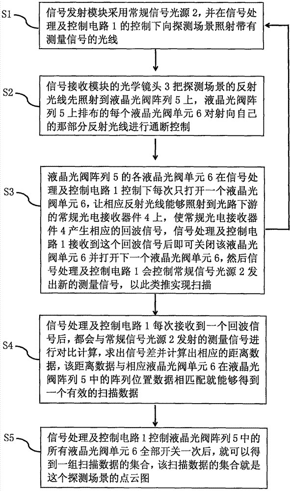
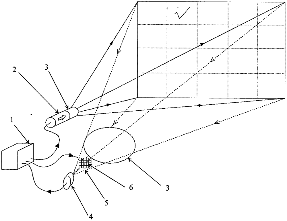
[0014] In order to make the above-mentioned purpose, features and advantages of the present invention more obvious and understandable, the specific implementation manners of the present invention will be described in detail below in conjunction with the accompanying drawings. Many specific details will be set forth in the following description, the purpose is to help those skilled in the art to more fully understand the present invention, but obviously those skilled in the art can use more specific details different from this embodiment without violating the connotation of the present invention. Therefore, the present invention is not limited to the specific embodiments disclosed below. For example, although the present invention describes the principle of the present invention with a liquid crystal light valve array, it does not mean that the present invention is limited to the use of a liquid crystal light valve array. Kerr cell arrays, MEMS micro-mirror chips, etc. also bel...


PUM


Abstract

An all-solid-state laser radar scanning method employs a routine signal light source to enforce surface irradiation of a detection field, a liquid crystal light valve array is employed to switch each liquid crystal light valve unit on the liquid crystal light valve array one by one on an optical path between the optical module of a signal receiving module and a routine photoelectric receiver, and the reflection light of the whole detection scene is divided into optical signals one by one so as to realize all-solid-state scanning. The all-solid-state laser radar scanning method can use the routine signal light source and the routine photoelectric receiver, solve the problem that a current all-solid-state laser radar scanning method must depend on various special scanning chips and have a wide application prospect.

Description

technical field [0001] The invention relates to a scanning method of an all-solid-state laser radar, which belongs to the field of photoelectric detection. Background technique [0002] The laser radar is composed of three parts: the signal transmitting module, the signal receiving module, the signal processing and the control circuit. Among them, the existing all-solid-state laser radar has two scanning schemes. One is to use the beam scanning laser chip in the signal transmitting module to deflect the beam. The optical scanning method of irradiation, and the other is to directly let the photoelectric units arranged in an array on the array photoelectric receiving chip electronically scan in the signal receiving module. Both of these methods need to rely on the above-mentioned special scanning chips. These special scanning chips are There are the problems of complex manufacturing process, low output and high cost. For example, Quanergy’s S3 optical phased array laser scann...

Claims


Application Information

Patent Timeline
Patent Type & Authority Applications(China)
IPC IPC(8): G01S7/481
CPCG01S7/4817
Inventor 陈明陈锋
Owner 陈明
Why Eureka
Try Eureka