Array substrate and liquid crystal display device

An array substrate and liquid crystal technology, applied in static indicators, nonlinear optics, instruments, etc., can solve the problem of low charging efficiency of pixel electrodes

Inactive Publication Date: 2017-10-20
BOE TECH GRP CO LTD +1
View PDF4 Cites 5 Cited by
  • Summary
  • Abstract
  • Description
  • Claims
  • Application Information

AI Technical Summary

Problems solved by technology

[0003] The invention provides an array substrate and a liquid crystal display device, which solves the technical problem of low charging efficiency of pixel electrodes of the existing array substrate compared with the prior art

Method used


Image

  • Array substrate and liquid crystal display device
  • Array substrate and liquid crystal display device
  • Array substrate and liquid crystal display device

Examples


Embodiment 1

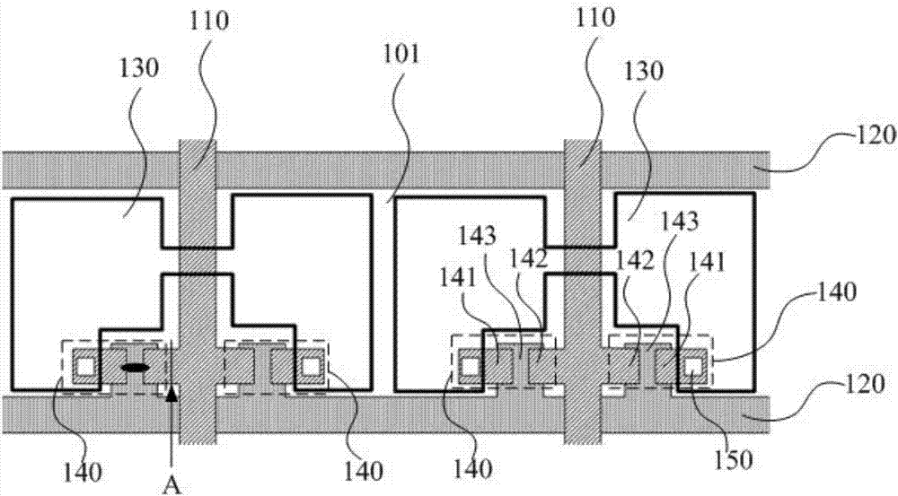
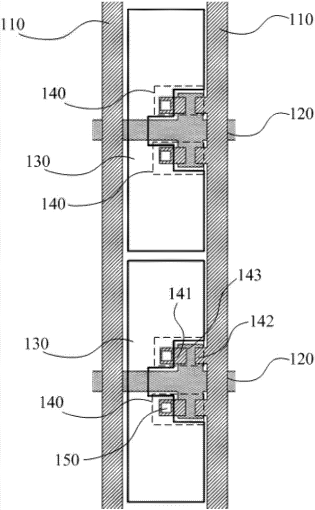
[0032] The array substrate of Embodiment 1 of the present invention, such as figure 1 and figure 2 As shown, it includes a plurality of parallel data lines 110 and a plurality of scan lines 120 vertically intersecting with the data lines, and the data lines 110 and the scan lines 120 are insulated at the intersections;

[0033] The array substrate further includes pixel electrodes 130 , and each pixel electrode 130 is driven by n thin film transistors 140 sharing the same data line and the same scan line, where n is a positive integer greater than or equal to 2.

[0034] The array substrate of this embodiment includes a plurality of parallel data lines and a plurality of scan lines vertically intersecting the data lines, and the data lines and the scan lines are insulated at the intersections; the array substrate also includes pixel electrodes, and each pixel electrode is shared by n Thin film transistor drives of the same data line and the same scan line. Since a pixel ele...

Embodiment 2

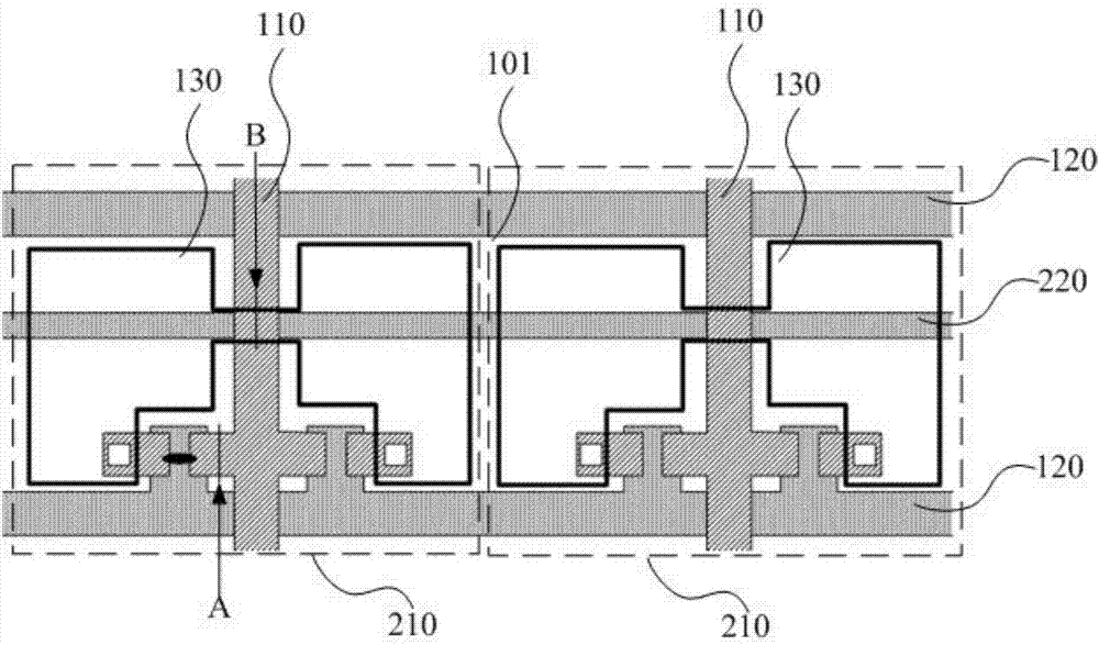
[0055] The array substrate of the second embodiment of the present invention, such as image 3 and Figure 4 shown, compared to figure 1 and figure 2 The difference between the array substrates shown is that the array substrate according to Embodiment 2 of the present invention also includes a common electrode 220 and a color filter layer; the color filter layer includes a pixel array and each pixel of the pixel array includes a plurality of sub-pixels 210;

[0056] The sub-pixels 210 correspond to the pixel electrodes 130 one by one; the voltage of the pixel electrodes 130 is adjusted to adjust the intensity of the electric field between the pixel electrodes 130 and the common electrode 220 .

[0057] Regarding the pixel, it may be a pixel including a red sub-pixel (R), a green sub-pixel (G) and a blue sub-pixel (B), or may be a pixel including a red sub-pixel (R), a green sub-pixel (G), a blue sub-pixel Sub-pixel (B) and white sub-pixel (W) pixels and so on.

[0058] Th...

Embodiment 3

[0061] Embodiment 2 of the present invention provides a liquid crystal display device, including a color filter substrate and an array substrate in a box, and liquid crystals filled between them; the array substrate described in either Embodiment 1 or Embodiment 2 Array substrate;

[0062] The intensity of the electric field between the pixel electrode and the common electrode is adjusted by adjusting the voltage of the pixel electrode, and then the deflection of the liquid crystal is controlled to control the brightness of the light of the sub-pixel corresponding to the pixel electrode.

[0063] In the liquid crystal display device of this embodiment, the intensity of the electric field between the pixel electrode and the common electrode is adjusted by adjusting the voltage of the pixel electrode, and then the deflection of the liquid crystal is controlled to control the sub-pixel corresponding to the pixel electrode. the brightness of the light. At the same time, there are...


PUM


Abstract

The invention discloses an array substrate and a liquid crystal display device. The array substrate comprises multiple parallel data cables and multiple scanning lines which perpendicularly insect with the data cables, and the data cables and the scanning lines are insulated at the junction; the array substrate further comprises pixel electrodes, and each pixel electrode is driven by n thin film transistors which share the same data cable and the same scanning line, wherein n is a positive integer larger than or equal to 2. The liquid crystal display device comprises the array substrate. According to the array substrate and the liquid crystal display device, compared with the prior art, the technical problem that pixel electrodes of an existing array substrate are low in charging efficiency is solved.

Description

technical field [0001] The invention relates to the field of liquid crystal display, in particular to an array substrate and a liquid crystal display device. Background technique [0002] In existing thin film transistor liquid crystal display devices, thin film transistors are key components. In order to achieve better display quality, it is necessary to continuously improve the characteristics of thin film transistors. Increasing the width-to-length ratio of the channel of the thin film transistor to increase the turn-on current of the thin film transistor is currently a research direction. However, the width-to-length ratio of the channel of the thin film transistor is limited by the manufacturing process of the thin film transistor, so the degree of increasing the turn-on current is limited, which leads to low charging efficiency of the pixel electrode. Contents of the invention [0003] The invention provides an array substrate and a liquid crystal display device. C...

Claims


Application Information

Patent Timeline
Patent Type & Authority Applications(China)
IPC IPC(8): G02F1/1362G02F1/1368G02F1/133
CPCG02F1/13306G02F1/136286G02F1/1368G02F1/1362G02F2202/10G02F1/13624G02F1/134336G02F2201/123G02F1/133514G02F1/134345
Inventor 王恺黄中浩史高飞
Owner BOE TECH GRP CO LTD
Why Eureka
Try Eureka