Silicon chip cutting device

A silicon wafer cutting and cutting knife technology, which is applied to fine working devices, working accessories, stone processing equipment, etc., can solve the problems of silicon wafer damage, waste, low cutting efficiency, etc., to avoid offset and reduce waste. Effect

Inactive Publication Date: 2017-10-24
安徽中柜智能科技有限公司
View PDF6 Cites 4 Cited by
  • Summary
  • Abstract
  • Description
  • Claims
  • Application Information

AI Technical Summary

Problems solved by technology

Among them, slicing is the process of cutting silicon rods into silicon wafers. In the cutting process, if the cutting is not accurate, there will be deviation during cutting, which will lead to low cutting efficiency, resulting in unnecessary waste and production. High cost; at the same time, for a single silicon wafer, if it cannot be cut successfully at one time and needs to be cut back and forth, it will cause unnecessary damage to the silicon wafer

Method used


Image

  • Silicon chip cutting device
  • Silicon chip cutting device
  • Silicon chip cutting device

Examples


Embodiment Construction

[0015] In order to have a further understanding and understanding of the structural features of the present invention and the achieved effects, the preferred embodiments and accompanying drawings are used for a detailed description, as follows:

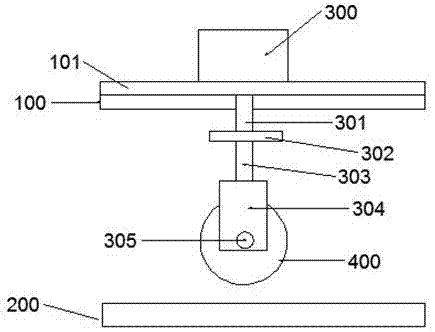
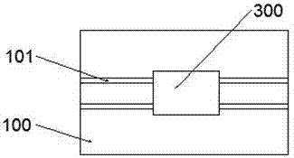
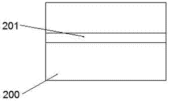
[0016] as attached Figure 1~3 As shown, the silicon wafer cutting device includes an upper support 100, a fixed table 200, a cylinder 300, and a cutting knife 400;

[0017] The upper bracket 100 is located above the fixed table 200, and the upper bracket 100 is provided with two slide rails 101, which are parallel to each other between the two slide rails 101, and the slide rails 101 and the fixed table 200 parallel to each other. The air cylinder 300 is horizontally arranged between the two slide rails 101, the telescopic end 301 of the air cylinder 300 is longitudinally arranged below the upper bracket 100, and the end of the telescopic end 301 close to the fixed table 200 is horizontally A push plate 302 is provided, the bottom ...


PUM


Abstract

A silicon wafer cutting device, including an upper bracket, a fixed table, a cylinder, and a cutting knife; the upper bracket is arranged above the fixed table, and two slide rails are arranged on the upper bracket, and the two slide rails are connected to each other. Parallel, the cylinder is horizontally arranged between the two slide rails, the telescopic end of the cylinder is vertically arranged below the upper bracket, and the end of the telescopic end close to the fixed table is horizontally provided with a push plate, The bottom of the push plate is longitudinally provided with a connecting rod, and the bottom of the connecting rod is fixed with a cutting knife fixing frame, and the cutting knife is arranged in the cutting knife fixing frame; a positioning cutting groove is horizontally arranged on the fixing platform. The beneficial effects of the present invention are as follows: (1) the cutting device can cut a single silicon chip at one time, avoiding back and forth cutting, resulting in damage to the silicon chip and irregularity of the edge of the silicon chip; (2) the fixed table is equipped with The positioning of the cutting groove avoids the deviation of the silicon wafer during cutting and reduces the waste of cost.

Description

technical field [0001] The invention belongs to the technical field of solar battery sheet preparation, and in particular relates to a silicon wafer cutting device. Background technique [0002] The process flow of solar panel production is slicing→cleaning→preparing suede→peripheral etching→removing the PN+ junction on the back→making upper and lower electrodes→making anti-reflection film→sintering→testing→grading. Among them, slicing is the process of cutting silicon rods into silicon wafers. In the cutting process, if the cutting is not accurate, there will be deviation during cutting, which will lead to low cutting efficiency, resulting in unnecessary waste and production. The cost is high; at the same time, for a single silicon wafer, if it cannot be cut successfully at one time and needs to be cut back and forth, it will cause unnecessary damage to the silicon wafer. Contents of the invention [0003] The object of the present invention is to provide a silicon wafer...

Claims


Application Information

Patent Timeline
Patent Type & Authority Applications(China)
IPC IPC(8): B28D5/02B28D7/04
CPCB28D5/023B28D5/0082
Inventor 孙文生孙传涛
Owner 安徽中柜智能科技有限公司
Why Eureka
Try Eureka