PCB-based GMI sensor probe and preparation method for the same

A sensor probe, PCB board technology, applied in the direction of instruments, single equipment manufacturing, measuring devices, etc., can solve the problems of difficulty in ensuring the number of coil turns and the stability of the winding diameter, time-consuming and laborious, and achieve flexible and convenient application and mature processing technology. Simple, technically mature effects

Inactive Publication Date: 2017-10-24
NAT UNIV OF DEFENSE TECH
View PDF11 Cites 2 Cited by
  • Summary
  • Abstract
  • Description
  • Claims
  • Application Information

AI Technical Summary

Problems solved by technology

Not only is it time-consuming and laborious, but it is also difficult to ensure the stability of the number of turns and winding diameter of the coil

Method used


Image

  • PCB-based GMI sensor probe and preparation method for the same
  • PCB-based GMI sensor probe and preparation method for the same

Examples


Embodiment Construction

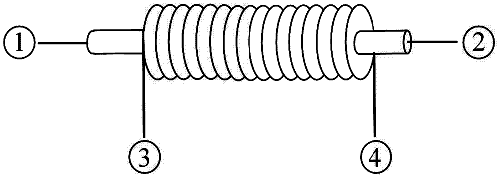
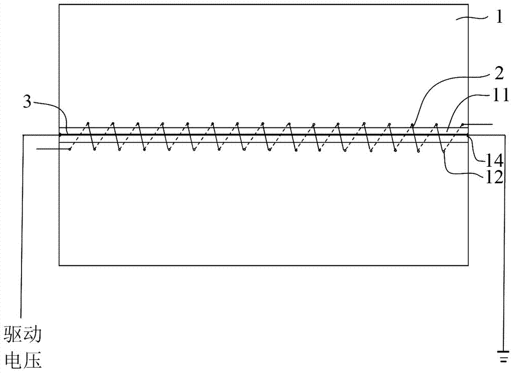
[0016] Such as figure 2 As shown, the GMI sensor probe based on PCB in this embodiment includes a PCB board 1 and a signal pickup coil 2. The PCB board 1 is provided with a groove 11 formed by etching, and the groove 11 is provided with an amorphous wire 3, and the PCB board 1 A row of via holes 12 are respectively provided on both sides of the groove 11 , and the signal pick-up coil 2 is formed by wires passing through the via holes 12 alternately on the front and back sides of the PCB 1 . In this embodiment, the signal pickup coil 2 is not a traditional coil coil, but a zigzag coil.

[0017] In this embodiment, both sides of the PCB board 1 are provided with stamp holes 14 for connecting drive signals, and the two ends of the amorphous wire 3 are respectively connected to the stamp holes 14. The packaging of the amorphous wire 3 is realized through the above structure, ensuring that the amorphous wire 3 The wire 3 connection is stable and reliable.

[0018] In this embodi...


PUM


Abstract

The present invention discloses a PCB-based GMI sensor probe and a preparation method for the same. The GMI sensor probe comprises a PCB and a signal pick-up coil, wherein the PCB is provided with an etching-formed groove; the groove is provided with amorphous wires; and the two sides of the PCB in the groove are provided with a row of through holes respectively. The signal pick-up coil is formed in such a way that the conductive wires pass the through holes sequentially and alternately winds on the front face and the back face of the PCB. The preparation method includes the following steps: etching the surface of the PCB to develop a groove; placing amorphous wires in the groove; forming two rows of through holes on both sides of the groove on the PCB; and forming a signal pick-up coil by letting the conductive wires pass the through holes sequentially and alternately wind on the front face and the back face of the PCB. The sensor probe and the preparation method for the same of the invention have the advantages of possessing a simple and stable process, are low in cost, flexible and convenient in application.

Description

technical field [0001] The invention relates to a biomagnetic signal acquisition device for brain-computer interface technology research experiments, in particular to a PCB-based GMI sensor probe and a preparation method thereof. Background technique [0002] In the field of magnetic measurement, GMI magnetic sensors have attracted wide attention due to their wide measurement range, high limit sensitivity and their convenience and ease of use. The GMI effect is when the wires or strips of soft magnetic materials (mostly Co-based amorphous and Fe-based nanocrystals) are fed with an alternating current I ac , the AC voltage induced across the material U w With the external magnetic field applied in the longitudinal direction of the wire H ex The phenomenon of sensitive change due to the change of the amorphous material itself is the sensitive change of the impedance of the amorphous material itself with the external magnetic field. Through the signal acquisition coil, we...

Claims


Application Information

Patent Timeline
IPC IPC(8): G01R33/09G01R33/00
CPCG01R33/0052G01R33/093
Inventor 徐明周宗潭郭善磁卢惠民肖军浩
Owner NAT UNIV OF DEFENSE TECH
Why Eureka
Try Eureka