LED device and display device comprising same

A technology of LED devices and LED chips, applied in the direction of electric solid devices, semiconductor devices, electrical components, etc., can solve the problems of low integration of backlight modules, and achieve the effect of improving the overall integration.

Pending Publication Date: 2017-10-31
ZHANGJIAGANG KANGDE XIN OPTRONICS MATERIAL
View PDF4 Cites 2 Cited by
  • Summary
  • Abstract
  • Description
  • Claims
  • Application Information

AI Technical Summary

Problems solved by technology

[0003] The main purpose of the present invention is to provide an LED device and a display device containing it to solve the problem of low integration of the backlight module of the display device in the prior art

Method used


Image

  • LED device and display device comprising same
  • LED device and display device comprising same
  • LED device and display device comprising same

Examples


Embodiment 1

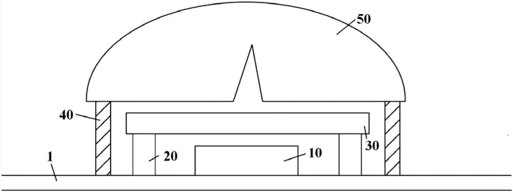
[0050] Such as figure 1 In the LED device shown, the LED is Sharp 3535LED, and a filter is set above the LED chip. The first colloid is thermosetting glue, and the filter is supported on the PCB. The setting method of the first colloid is as follows: Ring glue, the second glue is thermosetting glue, which supports the lens on the PCB, and the setting method of the second glue is ring glue. The shortest distance between the LED chip and the filter is 0.1mm, and the shortest distance between the filter and the above lens is 0.1mm. The geometric center of the above-mentioned LED chip coincides with the geometric center of the above-mentioned optical filter.

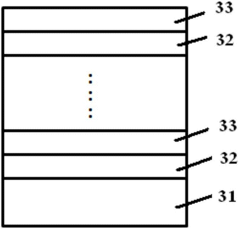
[0051] Using the physical deposition method, a ZnS layer, a cryolite layer, and a TiO layer were sequentially deposited on the surface of a PET substrate layer with a thickness of 50 μm and a total light transmittance of 90%. 2 layer, MgF 2 layer, Nb 2 o 5 layer, cryolite layer, Ta 2 o 5 layer, SiO 2 layer, ZnO layer...

Embodiment 2

[0053] Using the same method as in Example 1, a ZnS layer, a cryolite layer, a TiO 2 layer, MgF 2 layer, Nb 2 o 5 layer, cryolite layer, Ta 2 o 5 layer, SiO 2 layer, ZnO layer, MgF 2 layer, ZnS layer, cryolite layer, TiO 2 layer, MgF 2 layer, Nb 2 o 5 layer, cryolite layer, Ta 2 o 5 layer, SiO 2 layer, ZnO layer and MgF 2 layers, 10 first filter layers and 10 second filter layers, forming a filter. The first 10 filter layers arranged according to the deposition sequence are exactly the same (including material and thickness) as the last 10 filter layers, and the first 10 filter layers are exactly the same as the first 10 filter layers in Example 1.

Embodiment 3

[0055] The preparation method of the optical filter is the same as in Example 2, and the difference from Example 2 is that 5 first filter layers and 5 second filter layers are added, and these 10 additional filter layers are the same as those in Example 2. The order of setting the first 10 filter layers of 2 is exactly the same as that of the material.


PUM


Abstract

The invention provides an LED device and a display device comprising the same. The LED device comprises a printed circuit board (PCB) and a plurality of LEDs, wherein the plurality of LEDs are arranged on a surface of the PCB, each LED comprises an LED chip, an optical filter and a lens, the LED chip is arranged on the surface of the PCB, the optical filter is arranged at one side, far away from the PCB, of the LED chip and comprises a substrate layer and a filtering film, the substrate layer is arranged near to the LED chip, the filtering film is arranged at one side, far away from the LED chip, of the substrate layer, and the lens is arranged at one side, far away from the LED chip, of the optical filter. The optical filter is arranged in the LED, the comprehensive integration of a backlight module of the display device is improved, and the development trend of device size miniaturization is met.

Description

technical field [0001] The invention relates to the field of thin films, in particular to an LED device and a display device comprising it. Background technique [0002] In the prior art, the backlight module of the display device usually uses LED as the backlight source. In order to improve the color gamut of the display device, a filter is added to the backlight module. The filter is usually combined with other optical films in the backlight module (such as Diffusion sheets, prism sheets, etc.) are also arranged above the LEDs, such a backlight module is not highly integrated, and does not meet the industry's requirements for high integration of backlight modules. Contents of the invention [0003] The main purpose of the present invention is to provide an LED device and a display device including it, so as to solve the problem of low integration of the backlight module of the display device in the prior art. [0004] In order to achieve the above object, according to o...

Claims


Application Information

Patent Timeline
Patent Type & Authority Applications(China)
IPC IPC(8): H01L25/13H01L33/52H01L33/58
CPCH01L25/13H01L33/52H01L33/58
Inventor 李硕于甄高建聪谈俊
Owner ZHANGJIAGANG KANGDE XIN OPTRONICS MATERIAL
Why Eureka
Try Eureka