Thin composite circuit board
A composite circuit and flexible circuit board technology, applied in the directions of printed circuit, multi-layer circuit manufacturing, printed circuit manufacturing, etc., can solve the problem that the composite circuit board cannot be thinned, meet the requirements of reducing punching accuracy and improve thinning degree, the effect of simplifying the production process
- Summary
- Abstract
- Description
- Claims
- Application Information
AI Technical Summary
Problems solved by technology
Method used
Image
Examples
Embodiment 1
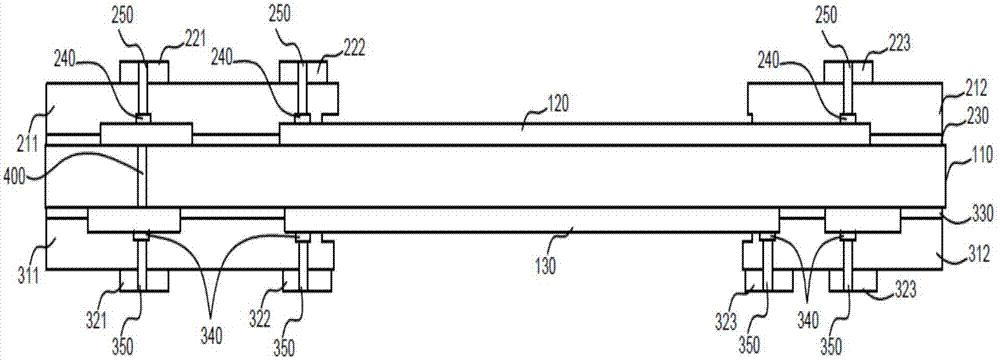
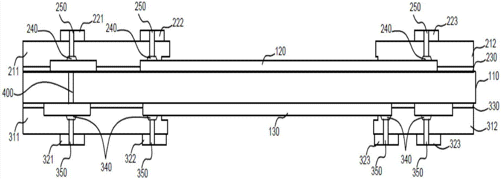
[0029] The invention provides a thin composite circuit board, such as figure 1 As shown, it includes: a flexible circuit board and a first rigid circuit board and a second rigid circuit board arranged on the upper and lower surfaces of the flexible circuit board. The flexible circuit board includes a flexible dielectric layer 110 and is arranged on the flexible circuit board. The first circuit layer 120 and the second circuit layer 130 on the upper and lower surfaces of the flexible dielectric layer 110, the first circuit layer 120 and the second circuit layer 130 are separated by the flexible dielectric layer 110, and the flexible dielectric layer One end of 110 is provided with at least one channel 400, and the two ends of the channel 400 respectively connect with the inner layers of the first circuit layer 120 and the second circuit layer 130 located at one end of the flexible circuit board, so that when the inner wall of the channel 400 is copper-plated, the second circuit ...
Embodiment 2
[0043] The difference from Embodiment 1 is that the outer diameter of the first connection hole 240 and the second connection hole 340 are smaller than the inner diameter. After the first rigid circuit board, the second rigid circuit board and the flexible circuit board are pressed together, the connection The hole will be deformed, and the diameter of the inside hole will be smaller than the outside hole diameter, and even the inside will be squeezed and closed. After copper plating, the conductive via hole connecting the outer layer circuit and the first circuit layer cannot be formed. Therefore, this embodiment connects each The hole is designed as a structure with a small outside and a large inside. Even after the first rigid circuit board, the second rigid circuit board and the flexible circuit board are pressed together, there are at least holes in the inner side of the connection hole, so that after copper plating, it can effectively form a connection outside. The first ...
PUM
 Abstract
Description
Claims
Application Information

