Patterning process

a patterning and material layer technology, applied in the direction of photosensitive materials, instruments, photomechanical treatment, etc., can solve the problems of complex process procedures and reduced throughput, and achieve the effect of reducing manufacturing costs and easy manufacturing procedures

Active Publication Date: 2009-05-21
MACRONIX INT CO LTD
View PDF7 Cites 37 Cited by
  • Summary
  • Abstract
  • Description
  • Claims
  • Application Information

AI Technical Summary

Benefits of technology

[0006]Accordingly, the present invention is to provide a method for patterning a material layer capable of providing relatively easy manufacturing procedure and decreasing manufacturing cost.

Problems solved by technology

However, in the conventional double patterning process, the etching process should be performed several times. Therefore, the process procedure is complex and the throughput is decreased.

Method used


Image

  • Patterning process
  • Patterning process
  • Patterning process

Examples


Embodiment Construction

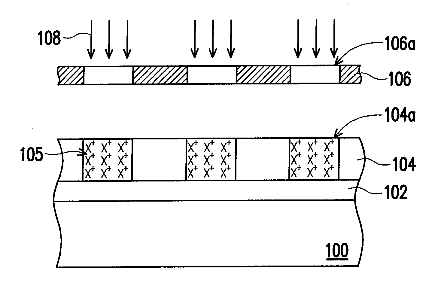
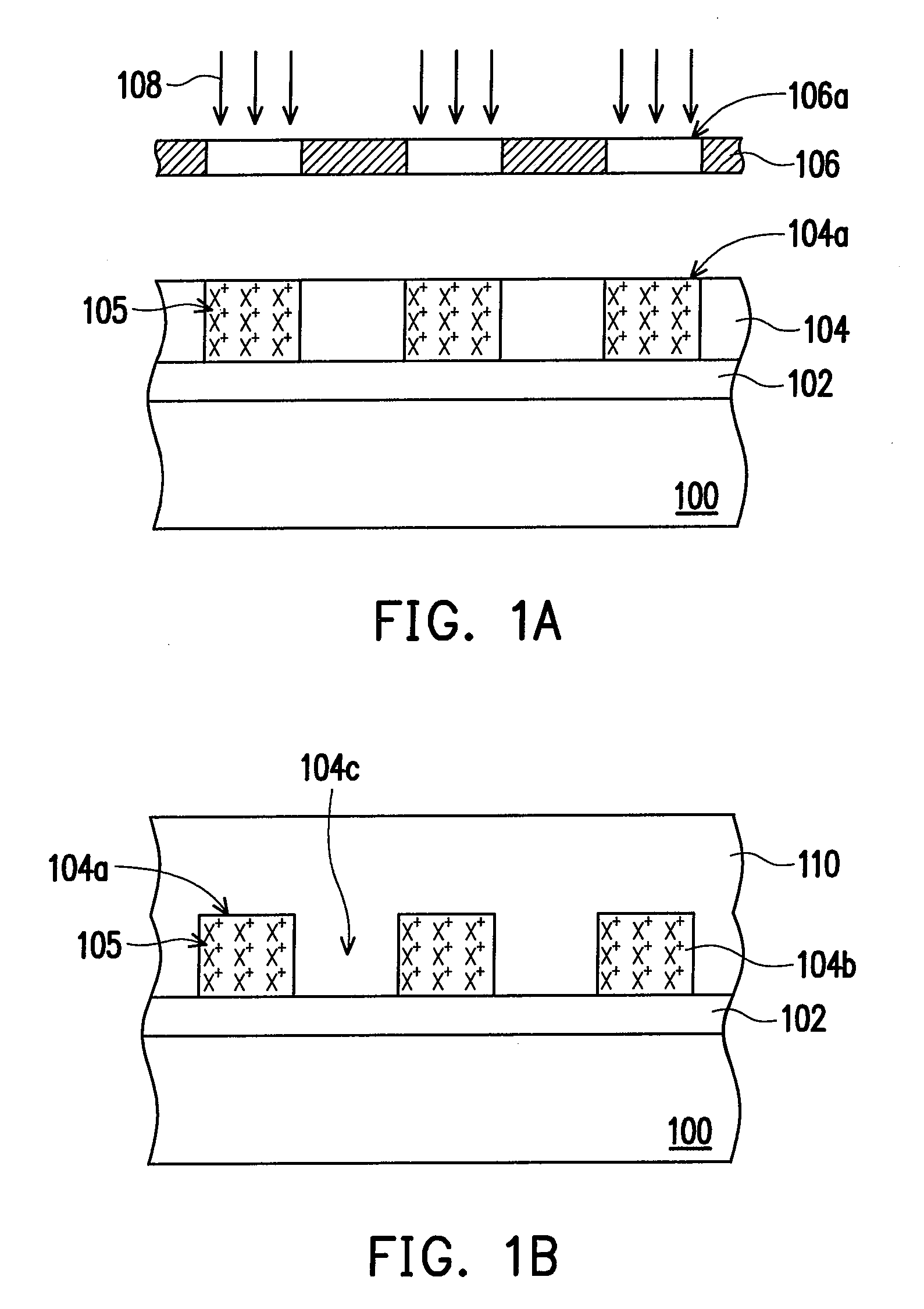
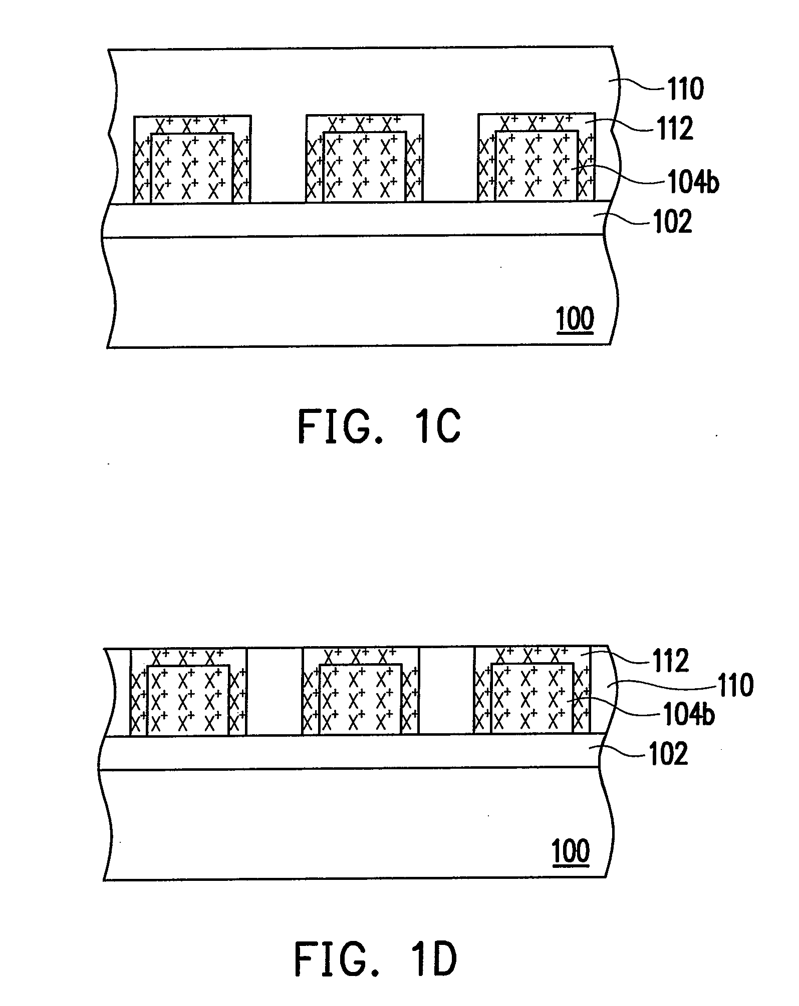
[0029]FIGS. 1A through 1F are schematic diagrams illustrating a method for patterning a material layer according to one embodiment of the present invention. As shown in FIG. 1A, a substrate 100 having a material layer 102 formed thereon is provided. It should be noticed that there are several interconnect layers (not shown) formed between the substrate 100 and the material layer 102, and the interconnect layers are not detail described herein. Then, a first mask layer 104 is formed over the substrate 100. Thereafter, an exposure process 108 is performed with the use of the photomask 106 having a pattern 106a. Hence, the pattern 106a of the photomask 106 is transformed into the first mask layer 104 as a pattern 104a. As shown in FIG. 1B, a develop process is performed to remove the unexposed portion of the first mask layer 104 and the exposed portion of the first mask layer 104, which is labeled 104b in FIG. 1B, remains on the material layer 102. In the present embodiment, the first ...


PUM

PropertyMeasurementUnit
temperatureaaaaaaaaaa
timeaaaaaaaaaa
developer-solubleaaaaaaaaaa

Abstract

The invention is directed to a method for patterning a material layer. The method comprises steps of forming a first mask layer on the material layer and then patterning the first mask layer. The patterned first mask layer has a pattern therein and a plurality of gaps within the patterns and the gaps expose a portion of the material layer. Further, a second mask layer is formed over the material layer and the second mask layer fills the gaps. An interface layer is formed between the patterned first mask layer and the second mask layer. A portion of the second material layer is removed until the top surface of the interface layer is exposed. The interface layer is removed to expose a portion of the material layer and the material layer is patterned by using the patterned first mask layer and the second mask layer as a mask.

Description

BACKGROUND OF THE INVENTION[0001]1. Field of Invention[0002]The present invention relates to a method for forming a semiconductor device. More particularly, the present invention relates to a method for patterning a material layer.[0003]2. Description of Related Art[0004]In the manufacture of integrated circuit, photolithography process is used to transfer patterns from a photo mask having customized circuit patterns to thin films formed on a wafer. The image transfer process comprises steps of forming a photoresist layer on a material layer, illuminating the photoresist layer through a photomask having the customized circuit patterns, developing the photoresist layer and then etching the material layer by using the patterned photoresist layer as a mask. Hence, the image transfer process is accomplished. For a well-manufactured integrated circuit product, the image transfer process mentioned above is performed several times to transfer the circuit patterns to each non-process layers...

Claims


Application Information

Patent Timeline
Patent Type & Authority Applications(United States)
IPC IPC(8): G03C1/72
CPCG03F7/40
Inventor YANG, CHIN-CHENG
Owner MACRONIX INT CO LTD
Why Eureka
Try Eureka