Display substrate and display apparatus

A technology for display substrates and display devices, which is applied to semiconductor devices, electrical components, transistors, etc., can solve the problems of inability to provide signals from display panels, limited display panels, short-circuiting of pads, etc. Avoid short circuits and facilitate the effect of narrow borders

Inactive Publication Date: 2017-11-10
WUHAN TIANMA MICRO ELECTRONICS CO LTD
View PDF7 Cites 12 Cited by
  • Summary
  • Abstract
  • Description
  • Claims
  • Application Information

AI Technical Summary

Problems solved by technology

However, the bezel area of ​​the display panel is limited, so the spacing between adjacent pads will be reduced accordingly
Once a static charge is introduced on a certain pad, it will easily cause a short circuit between adjacent pads due to electrostatic breakdown, which will cause the subsequent integrated circuit to fail to provide signals to the display panel normally.

Method used


Image

  • Display substrate and display apparatus
  • Display substrate and display apparatus
  • Display substrate and display apparatus

Examples


Embodiment Construction

[0026] The application will be further described in detail below with reference to the drawings and embodiments. It can be understood that the specific embodiments described here are only used to explain the related invention, but not to limit the invention. In addition, it should be noted that, for ease of description, only the parts related to the invention are shown in the drawings.

[0027] It should be noted that the embodiments in the application and the features in the embodiments can be combined with each other if there is no conflict. Hereinafter, the present application will be described in detail with reference to the drawings and in conjunction with embodiments.

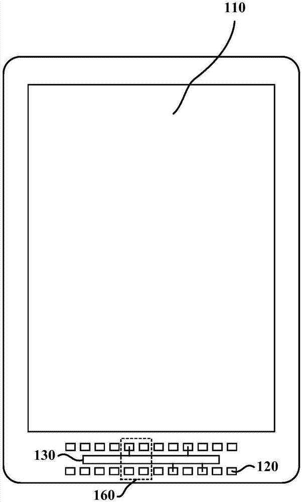
[0028] See figure 1 As shown, this is a schematic structural diagram of an embodiment of the display substrate of this application.

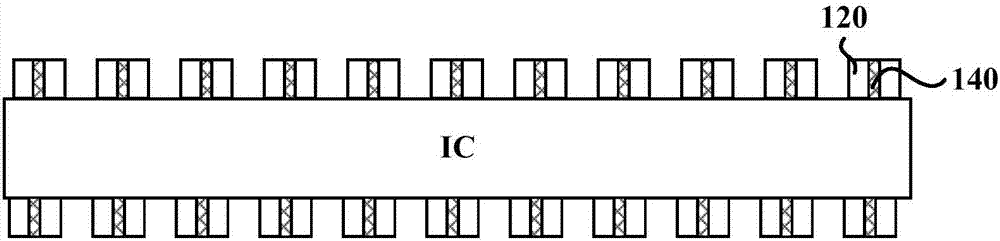
[0029] The display substrate of this embodiment includes a display area 110 and a non-display area surrounding the display area.

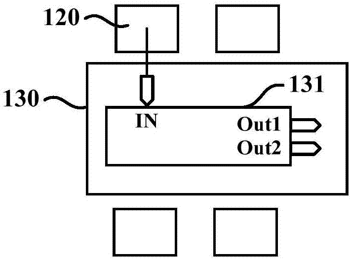
[0030] Among them, the non-display area is prov...


PUM


Abstract

The invention discloses a display substrate and a display apparatus. The display substrate includes a display area and a non-display area surrounding the display area, further includes a plurality of pads arranged on the non-display area, and an electrostatic protection circuit, wherein the pads and the pins of a display chip are correspondingly and electrically connected one by one, the electrostatic protection circuit is electrically connected with at least one pad for outputting the static electricity of the pad, the electrostatic protection circuit forms in the bonding area for bonding the display chip. According to the scheme, the at least one pad is electrically connected with the electrostatic protection circuit for outputting the static electricity of the pad, so that the short circuit caused by the static breakdown between the adjacent pads can be prevented, the electrostatic protection capability of the display substrate and the display device including the same is improved, and the manufacturing yield rate and the use reliability of the display substrate and the display device including the same are improved.

Description

Technical field [0001] The present disclosure generally relates to the field of display technology, and more particularly to a display substrate and a display device. Background technique [0002] Electro-Static Discharge (ESD, Electro-Static Discharge) is due to the large accumulation of static electricity during the process of display panel manufacturing. During the charge transfer process, it encounters thinner traces or intersecting lines, and the instantaneous current is too large. This kind of destruction phenomenon. [0003] With the increasing demand for PPI (Pixel per Inch), the size of the device is getting smaller and smaller, the line width of the metal and the distance between the metal and the metal are getting smaller and smaller. At the same time, the number of signal channels required by the display panel is also increasing, which also leads to an increase in the number of pins of integrated circuits that provide signals to the display panel. As a result, the num...

Claims


Application Information

Patent Timeline
Patent Type & Authority Applications(China)
IPC IPC(8): H01L27/02H01L27/12
CPCH01L27/0266H01L27/1214
Inventor 郑超杨康鹏许育民
Owner WUHAN TIANMA MICRO ELECTRONICS CO LTD
Why Eureka
Try Eureka