Supercharge Your Innovation With Domain-Expert AI Agents!

Air gap over transistor gate and related method

A technology of transistors and air gaps, applied in the field of semiconductor devices, can solve problems such as adverse effects

Active Publication Date: 2017-12-01
GLOBALFOUNDRIES U S INC MALTA
View PDF3 Cites 4 Cited by
  • Summary
  • Abstract
  • Description
  • Claims
  • Application Information

AI Technical Summary

Problems solved by technology

[0003] One challenge in forming RF switches in SOI substrates is controlling two conflicting parameters: the on-resistance (R on ), the resistance of the switch when the power is on; and the off-state capacitance (C off ), which represents the amount of crosstalk or noise that may occur within the system, that is, the amount by which a signal transmitted on one circuit adversely affects another circuit

Method used


Image

  • Air gap over transistor gate and related method
  • Air gap over transistor gate and related method
  • Air gap over transistor gate and related method

Examples


Embodiment Construction

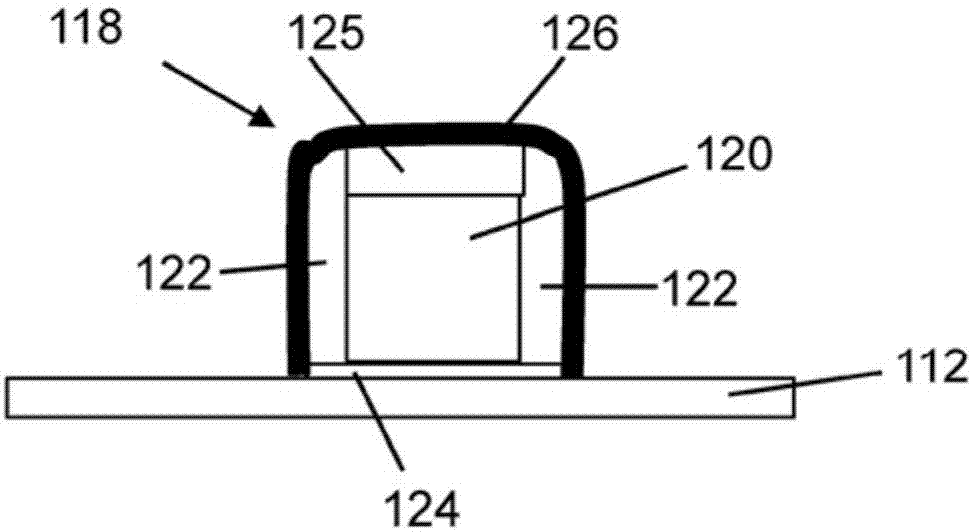
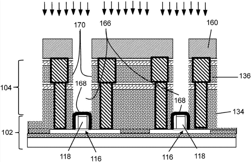
[0061] The present invention relates to a method of forming a semiconductor device that includes an air gap over a transistor gate to reduce the distance between the transistor gate and adjacent lines, contacts, and vias that contact the transistor's source and drain. of capacitance. This reduction in capacitance reduces the off-state capacitance of the transistor when it is used in applications such as radio frequency (RF) switching in semiconductor-on-insulator (SOI) substrates or bulk (non-SOI) substrates. By controlling one of the main factors of intrinsic field effect transistor (FET) capacitance: the effective dielectric constant of the contact or local interconnect layer and the first metal layer, various embodiments in accordance with the present invention use The air gap above the gate provides a mechanism to reduce the off-state capacitance of any device using the air gap. Although the teachings of the present invention will be described with respect to SOI substrat...


PUM


Abstract

The invention relates to an air gap over transistor gate and a related method. A semiconductor device may include a transistor gate in a device layer; an interconnect layer over the device layer; and an air gap extending through the interconnect layer to contact an upper surface of the transistor gate. The air gap provides a mechanism to reduce both on-resistance and off-capacitance for applications using SOI substrates such as radio frequency switches.

Description

technical field [0001] The present invention relates to semiconductor devices, and more particularly to an air gap over a gate of a transistor and a method for forming the same. This air gap reduces the off-state capacitance (C off ). Background technique [0002] Radio frequency (radio frequency; RF) switches are widely used in telecommunication devices such as smartphones to route high frequency telecommunication signals through transmission paths. For example, RF switches are commonly used in smartphones to allow the use of different digital wireless technology standards in different terrains. Current RF switches are typically fabricated using semiconductor-on-insulator (SOI) substrates. Typically, SOI substrates use layered silicon-insulator-silicon substrates instead of more traditional silicon substrates (bulk substrates). SOI-based devices differ from conventional silicon-built devices in that the silicon junction sits on top of an electrical insulator, typically ...

Claims


Application Information

Patent Timeline
Patent Type & Authority Applications(China)
IPC IPC(8): H01L23/482H01L21/336H01L29/78
CPCH01L23/4821H01L29/66477H01L29/78H01L23/53223H01L23/53238H01L23/53295H01L21/7682H01L23/485H01L23/5222H01L27/1203H01L23/5226
Inventor Z-X·贺马克·D·贾菲兰迪·L·沃夫亚文·J·乔瑟夫布莱特·T·古奇安东尼·K·史塔佩尔
Owner GLOBALFOUNDRIES U S INC MALTA
Features
  • R&D
  • Intellectual Property
  • Life Sciences
  • Materials
  • Tech Scout
  • Unparalleled Data Quality
  • Higher Quality Content
  • 60% Fewer Hallucinations
Learn More