Embedded fan-out type silicon pinboard applied to three-dimensional system-level packaging and manufacturing method

A system-in-package, fan-out technology, applied in semiconductor/solid-state device manufacturing, electrical components, electrical solid-state devices, etc., can solve problems such as the inability to further meet the application of multi-layer three-dimensional systems, reduce production costs, and improve product reliability. The effect of shortening the process flow

Pending Publication Date: 2017-12-08
XIAMEN UNIV
View PDF8 Cites 32 Cited by
  • Summary
  • Abstract
  • Description
  • Claims
  • Application Information

AI Technical Summary

Problems solved by technology

However, as the structural design becomes more and more complex and the performance requirements become higher and higher, eSiFO technology cannot further meet the requirements of complex multi-layer 3D system applications in smaller package sizes.

Method used


Image

  • Embedded fan-out type silicon pinboard applied to three-dimensional system-level packaging and manufacturing method
  • Embedded fan-out type silicon pinboard applied to three-dimensional system-level packaging and manufacturing method
  • Embedded fan-out type silicon pinboard applied to three-dimensional system-level packaging and manufacturing method

Examples


Embodiment 1

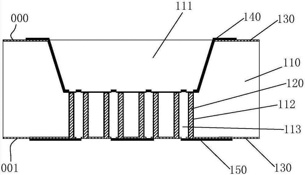
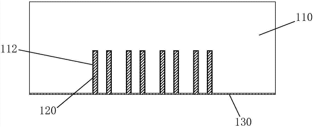
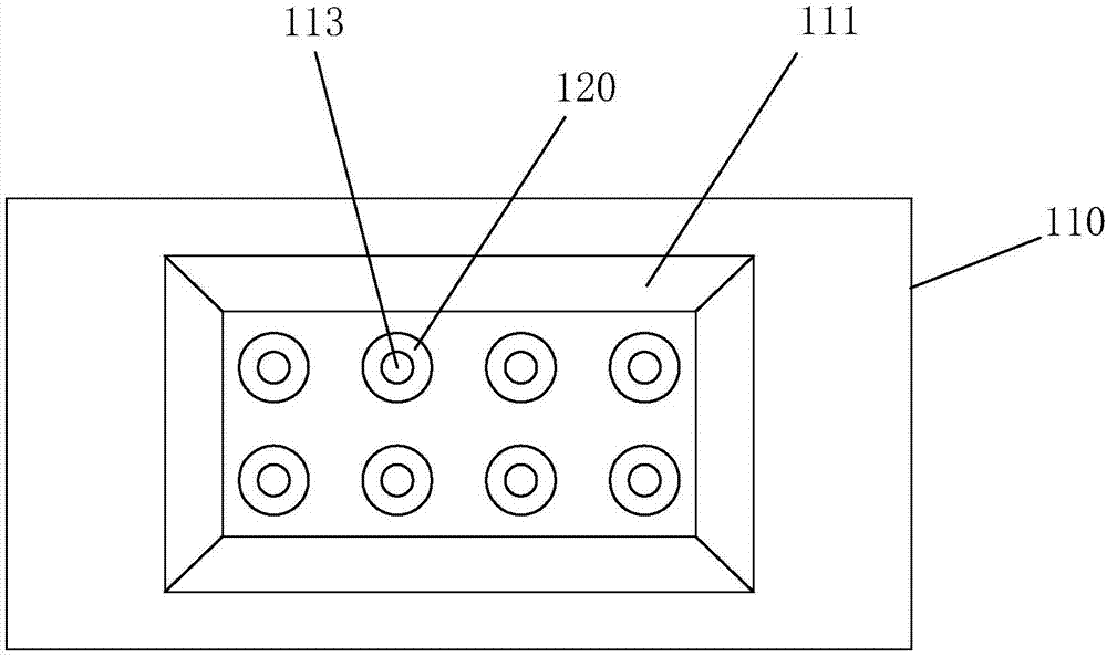
[0046] A new type of embedded fan-out silicon interposer structure for 3D system-in-package applications such as figure 1As shown, it includes a silicon substrate 110 made of low-resistance silicon material (≤0.1Ω·cm). The silicon substrate 110 has a front surface 000 and a back surface 001. The diameter of the cavity 111 gradually decreases from the front to the back), and the back is provided with a vertical interconnection structure extending to the bottom of the cavity 111 . The vertical interconnection structure is formed by the following structure: the back surface 001 of the silicon substrate 110 is provided with several annular grooves 112 extending to the bottom of the cavity 111 and independent of each other, and the annular grooves 112 are filled with insulating materials to form an annular insulating layer 120 The silicon pillars within the inner ring of the annular insulating layer 120 form conductive pillars 113 , that is, several mutually independent conductive ...

Embodiment 2

[0064] A new type of embedded fan-out silicon interposer structure for 3D system-in-package applications such as Figure 6 As shown, it includes a silicon substrate 210 made of high-resistance silicon material (≥1000Ω·cm). The silicon substrate 210 has a front surface 000 and a back surface 001. The front surface is provided with a concave cavity 211 (preferably concave The diameter of the cavity 211 gradually decreases from the front to the back), and the back is provided with a vertical interconnection structure extending to the bottom of the cavity 211. The vertical interconnect structure is formed by the following structure: the back of the silicon substrate 210 is provided with a plurality of through holes 212 extending to the bottom of the cavity 211 and independent of each other, and the through holes 212 are filled with conductive materials to form the conductive pillars 220 . The front and back of the silicon substrate 210 and the surface of the concave cavity are pro...


PUM


Abstract

The invention discloses an embedded fan-out type silicon pinboard applied to three-dimensional system-level packaging. The front side of a silicon substrate is provided with a concave cavity whose side wall has certain gradient, the reverse side is provided with a vertical interconnection structure extending to the bottom of the concave cavity, and the vertical interconnection structure includes a plurality of mutually independent conductive columns; the front side of the silicon substrate and the side wall and the bottom of the concave cavity are provided with first metal interconnection layers used for being connected with a microelectronic chip bonding pad placed in the concave cavity and manufacturing a front side leading-out end; and the reverse side of the silicon substrate is provided with a second metal interconnection layer to be used for manufacturing a reverse side leading-out end, the first metal interconnection layers and the second metal interconnection layer are insulated from the silicon substrate, and the conductive columns are electrically connected with the first metal interconnection layers and the second metal interconnection layer. The invention also discloses a manufacturing method of the embedded fan-out type silicon pinboard and application to packaging, by use of the concave cavity combined with the vertical interconnection structure, application to three-dimensional system packaging is further realized on the basis of meeting requirements of high density, small size and low cost, thereby improving product performance.

Description

technical field [0001] The invention relates to the field of microelectronic packaging, and more specifically relates to a novel embedded fan-out silicon adapter board structure and a manufacturing method for three-dimensional system-level packaging applications. Background technique [0002] With the rapid development of the integrated circuit manufacturing industry, the chip size is developing in the direction of higher density, faster speed, smaller size, and lower cost. The traditional fan-in wafer-level packaging can no longer meet the requirements of interconnection. However, Fan-out wafer-level packaging has the advantages of miniaturization, low cost and high integration, so fan-out wafer-level packaging (FOWLP) has emerged, which is most suitable for high-demand mobile or wireless markets, and further promotes The development of high-performance, small-size market. [0003] Infineon invented the fan-out wafer-level packaging (FOWLP) patent in 2004, and proposed the...

Claims


Application Information

Patent Timeline
Patent Type & Authority Applications(China)
IPC IPC(8): H01L23/13H01L23/538H01L21/768
CPCH01L23/5384H01L23/5386H01L21/76898H01L23/13H01L2924/15156H01L2924/15311H01L2924/18161H01L2224/16225
Inventor 马盛林蔡涵李继伟罗荣峰颜俊龚丹夏雁鸣秦利锋王玮陈兢金玉丰
Owner XIAMEN UNIV
Why Eureka
Try Eureka