Electromagnetic shielding package and manufacturing method

A technology of electromagnetic shielding and shielding body, which is applied in semiconductor/solid-state device manufacturing, electric solid-state devices, circuits, etc. It can solve the problems of unfavorable heat dissipation, high cost, and complexity of plastic packaging layers, and achieve simple manufacturing, elimination of electromagnetic interference, and good electromagnetic The effect of isolation

Active Publication Date: 2019-11-01
NAT CENT FOR ADVANCED PACKAGING CO LTD
View PDF4 Cites 0 Cited by
  • Summary
  • Abstract
  • Description
  • Claims
  • Application Information

AI Technical Summary

Problems solved by technology

The disadvantage of this solution is that it is a high-cost and complicated process to equip each chip with a large-area plastic packaging layer covering the entire chip. In addition, the plastic packaging layer is not conducive to heat dissipation.

Method used


Image

  • Electromagnetic shielding package and manufacturing method
  • Electromagnetic shielding package and manufacturing method
  • Electromagnetic shielding package and manufacturing method

Examples


Embodiment Construction

[0035] It should be noted that the components in the drawings may be exaggeratedly shown for illustration purposes, and not necessarily in correct proportions. In the drawings, the same reference numerals are assigned to the same or the same components.

[0036] Unless otherwise specified, in this application, the quantifiers "one" and "one" do not exclude scenarios with multiple elements.

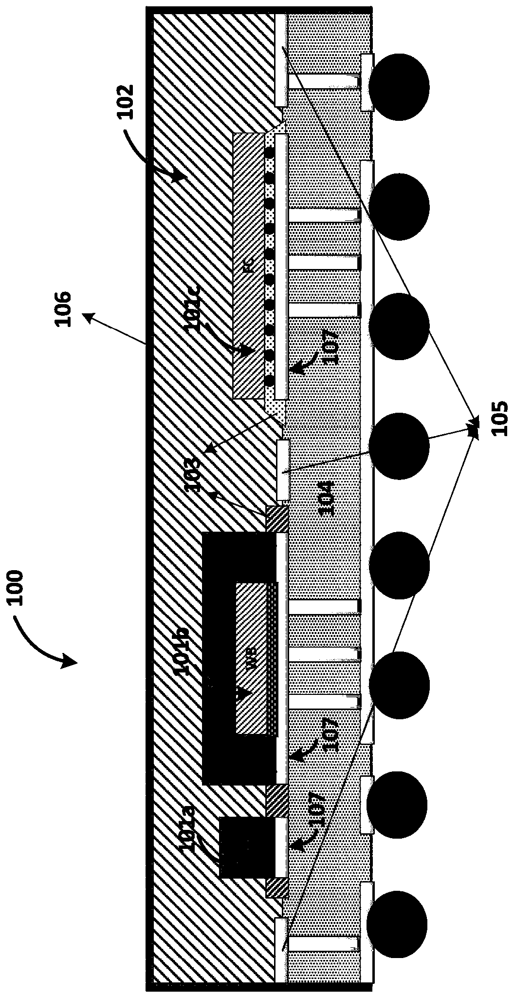
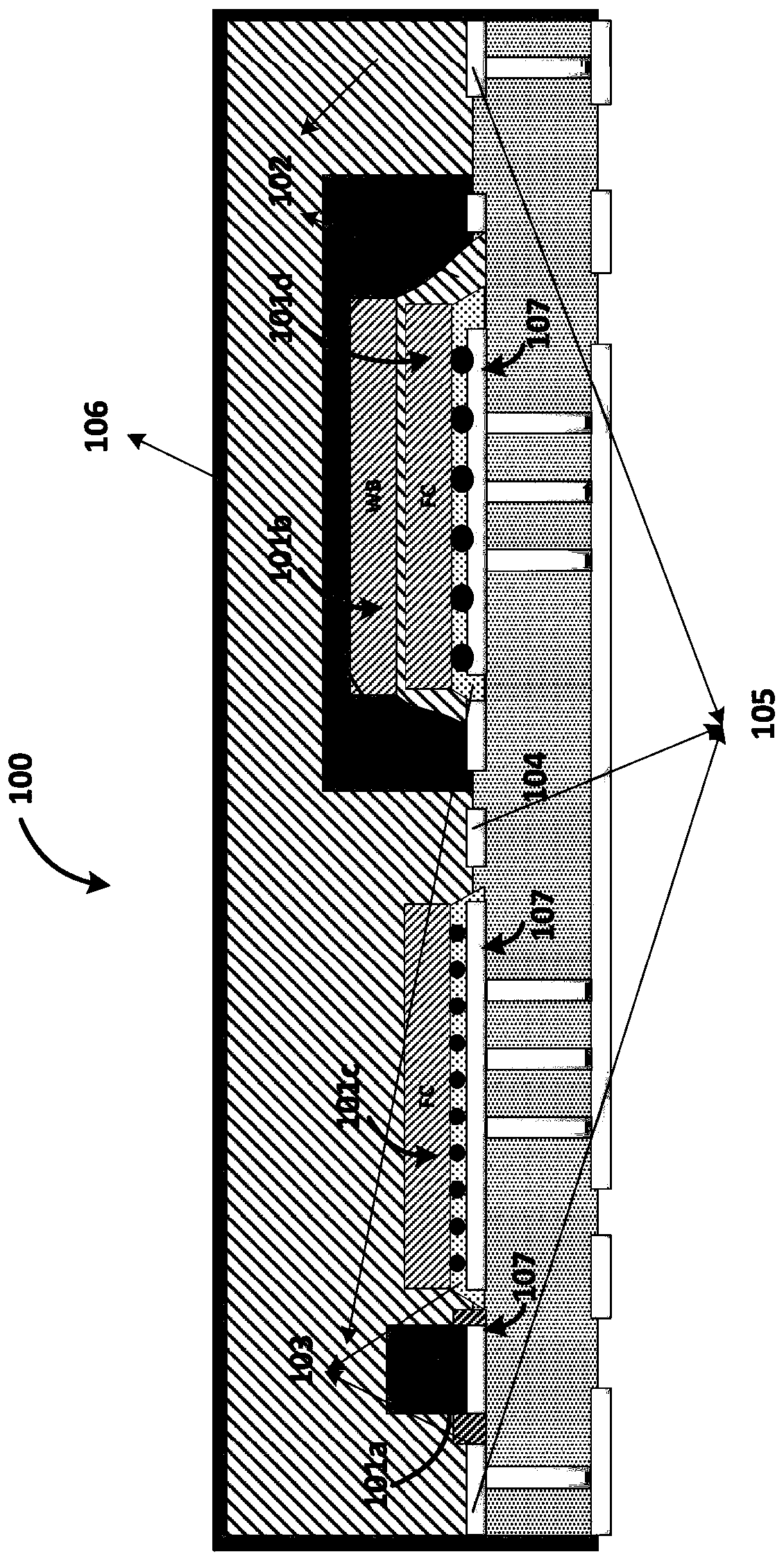
[0037] figure 1 A schematic diagram of the first embodiment of the electromagnetic shielding package 100 according to the present invention is shown.

[0038] Such as figure 1 As shown, the electromagnetic shielding package 100 includes a substrate 104. The substrate 104 may be, for example, a common printed circuit board (PCB). The substrate 104 may include various conductive structures, such as interconnection lines 107 for connecting the chips 101a, 101b, and 101c, and a grounding line 105 for grounding the shield 102, or may also include vias (not shown). These conductive structures can be...


PUM


Abstract

The invention relates to an electromagnetic shielding package, comprising: a substrate; at least two chips arranged on the substrate; a shield made of shielding glue, the shield covers the chips and isolates the chips from each other for use for electromagnetically shielding the chip from the environment and from each other, wherein the shield is grounded through a conductor; and an insulating layer made of insulating glue, wherein the insulating layer is applied on the chip where it should be in contact with the shield The electrically insulating conductive structure of the body and / or the conductive structure of the substrate which should be electrically insulated from the shielding body for electrically insulating said conductive structure from the shielding body. The invention also relates to a method for manufacturing such an electromagnetic shielding package.

Description

Technical field [0001] The present invention relates to the field of semiconductor manufacturing, and in particular to an electromagnetic shielding package and a method for manufacturing such a package. Background technique [0002] As the requirements for the portability, low weight, and small size of electronic products continue to increase, system-in-package (SiP) technology is booming. An important development trend of system-in-package is to package different chips such as high-speed digital circuits, analog circuits, and radio frequency circuits in a package to achieve the required integration. However, this creates the problem of electromagnetic interference between the chips in the package and the problem of electromagnetic radiation outside the package. [0003] One solution to the electromagnetic radiation problem is to use a metal shield. Such a shielding cover is usually composed of a frame with an isolation wall and a cover. The isolation wall is used to reduce elect...

Claims


Application Information

Patent Timeline
Patent Type & Authority Patents(China)
IPC IPC(8): H01L23/31H01L23/552H01L21/50H01L21/56
CPCH01L23/552H01L21/50H01L21/56H01L23/3114H01L23/3128H01L2924/181H01L2924/19105H01L2224/16225H01L2224/32145H01L2224/48091H01L2224/73204H01L2224/73265H01L2924/00014H01L2924/00012
Inventor 李君张绪
Owner NAT CENT FOR ADVANCED PACKAGING CO LTD
Why Eureka
Try Eureka