

Balance-to-unbalance signal filtering power divider
A signal filtering and unbalanced technology, which is applied in the direction of waveguide devices, circuits, connecting devices, etc., can solve the problems of large size, insufficient common mode suppression, and complex structure of filter power splitters.
- Summary
- Abstract
- Description
- Claims
- Application Information
AI Technical Summary
Problems solved by technology
Method used
Image

Examples
Embodiment 1
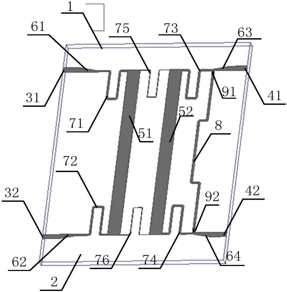
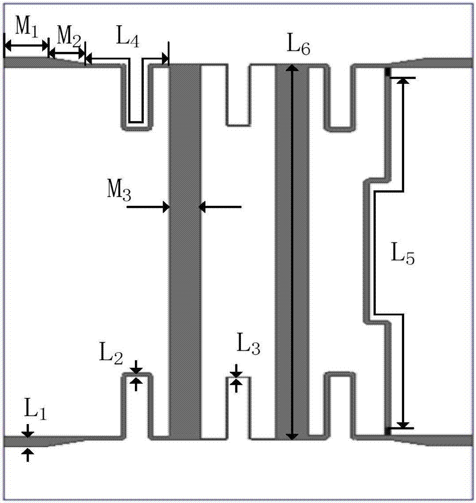
[0054] The three-dimensional structure of a balanced-to-unbalanced signal filter power splitter is as follows: figure 1 As shown, the relevant dimensions and specifications are as follows figure 2 shown. The dielectric substrate 20 used has a relative permittivity of 3.55, a thickness of 2 mm, and a loss tangent of 0.0027. combine figure 2 , The various dimensions of the power divider are as follows: M1=4mm, M2=4mm, M3=3mm, L1=1.2mm, L2=0.2mm, L3=0.1mm, L4=21.96mm, L5=44.67mm, L6=43.78 mm. The entire structure is arranged axisymmetrically with respect to the midline of the long sides of the dielectric substrate 20 .
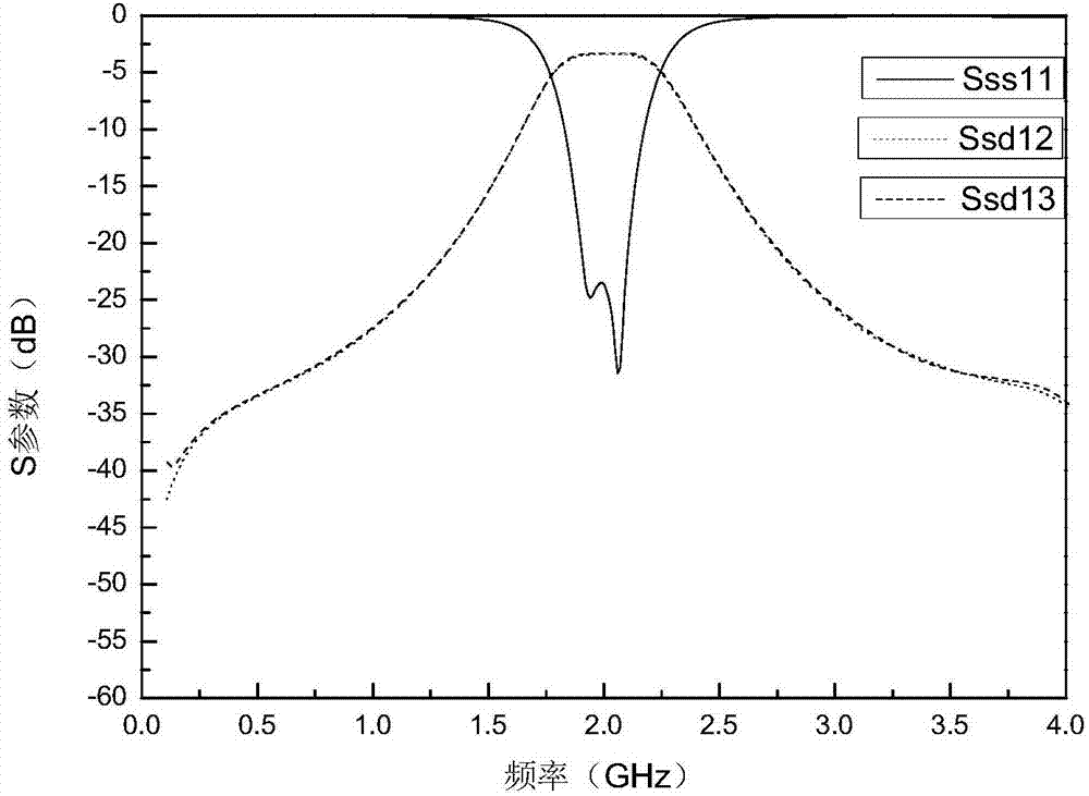
[0055] The power splitter of this example is modeled and simulated in the electromagnetic simulation software HFSS.13.
[0056] image 3 It is the S-parameter simulation diagram when the differential mode signal is input in the embodiment. It can be seen that the center frequency of the power divider is 2 GHz, and the square coefficient is very high, whi...
PUM
| Property | Measurement | Unit |
|---|---|---|
| Thickness | aaaaa | aaaaa |
Abstract
Description
Claims
Application Information