Oxide semiconductor film transistor trap state density extraction method

A technology of oxide semiconductors and thin film transistors, which is applied in the field of trap state density extraction of oxide semiconductor thin film transistors, and can solve problems such as changes in trap state distribution, difficult extraction of oxide semiconductor thin film transistors, and changes in material properties.

Active Publication Date: 2017-12-15
SUN YAT SEN UNIV
View PDF7 Cites 11 Cited by
  • Summary
  • Abstract
  • Description
  • Claims
  • Application Information

AI Technical Summary

Problems solved by technology

2) Field effect (F-E) method: This method assumes that the conduction mechanism of the transistor is mainly trap state-limited conduction. The existence of this prerequisite makes it difficult to extract the acceptor trap state of the oxide semiconductor thin film transistor.
However, light will change the material properties and change the distribution of trap states
4) Use the Mel-Nedo principle to extract, but the flat-band voltage and the Mel-Nedo factor of the transistor need to be known in advance. In addition, this method can only be used when the device works in the sub-threshold region

Method used


Image

  • Oxide semiconductor film transistor trap state density extraction method
  • Oxide semiconductor film transistor trap state density extraction method
  • Oxide semiconductor film transistor trap state density extraction method

Examples


Embodiment 1

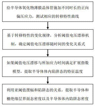
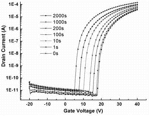
[0037] The object of the present invention is to provide a method for extracting the trap state density of oxide semiconductor thin film transistors, by measuring the transfer characteristic curves of oxide semiconductor thin film transistors under different time-length positive bias stresses at room temperature, if the threshold voltage drift and the applied stress time meet By extending the exponential model, the bulk state and interface state densities of thin film transistors can be calculated. The flowchart of the method is shown in figure 1 . The characteristic temperature of the trap state in the semiconductor body is extracted through the relationship between the threshold voltage drift and the time of the applied stress. obtained by calculation.

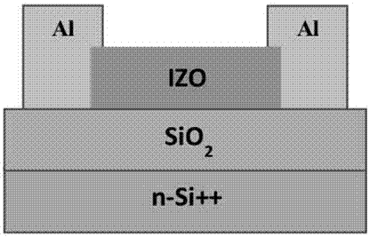
[0038]The specific embodiment of the present invention one is to adopt the trap state density extraction method of the oxide semiconductor thin film transistor provided by the present invention to extract the IZO / SiO of th...


PUM


Abstract

The invention relates to an oxide semiconductor film transistor trap state density extraction method, belongs to the technical field of a semiconductor device and includes semiconductor and gate insulation layer interface trap state extraction and internal trap state extraction of a semiconductor. The method comprises steps that (1), forward bias stresses with different durations are applied to an oxide semiconductor film transistor, and a corresponding transfer characteristic curve is tested; 2), based on transfer characteristic change rules, a threshold voltage drift mechanism is analyzed, and the change relation of the threshold voltage drift along with the time is determined; 3), if the threshold voltage drift and the applied stress time satisfy an expansion index model, characteristic temperature of an internal trap state of the semiconductor is extracted; and 4), the relationship between sub threshold amplitude and the trap state is utilized, semiconductor and gate insulation layer interface state density and internal trap state density of the semiconductor are extracted. The method is advantaged in that the film transistor interface trap state and the internal trap state can be simultaneously extracted, the calculation process is simpler compared with methods in the prior art, restriction conditions are a few, and the application scope is wide.

Description

technical field [0001] The present invention relates to the technical field of semiconductors, and more specifically, to a method for extracting trap state density of an oxide semiconductor thin film transistor. Background technique [0002] Oxide semiconductor thin film transistors have the advantages of high mobility, transparency, compatibility with the low-temperature preparation process of amorphous silicon, flexible display, and good uniformity in large-area production. They have attracted great attention and are widely used in AMLCD and AMOLED. , logic gates for ring oscillators, sensors, etc. [0003] The trap states of thin film transistors include the trap states at the interface between the semiconductor and the gate insulating layer and the trap states in the semiconductor body. Similar to hydrogenated amorphous silicon thin film transistors, oxide semiconductor thin film transistors also have more non-uniformly distributed bandgap defect states. These bandgap s...

Claims


Application Information

Patent Timeline
Patent Type & Authority Applications(China)
IPC IPC(8): G01R31/26
CPCG01R31/2648
Inventor 强蕾裴艳丽王钢
Owner SUN YAT SEN UNIV
Why Eureka
Try Eureka