FPGA chip, high-speed interface interconnection system and interconnection achieving method

A high-speed interface and interconnection system technology, applied in CAD circuit design, special data processing applications, instruments, etc., can solve problems such as easy failure, difficult debugging, chip design transplanted to a single FPGA chip, etc., to improve the success rate , Speed ​​up the debugging process and shorten the chip development cycle

Active Publication Date: 2017-12-15
SUZHOU LANGCHAO INTELLIGENT TECH CO LTD
View PDF4 Cites 6 Cited by
  • Summary
  • Abstract
  • Description
  • Claims
  • Application Information

AI Technical Summary

Problems solved by technology

[0005] In the chip FPGA prototype verification process, due to the increasing scale of chip design, it is impossible to transplant the entire design of the chip to a single FPGA chip. Therefore, it is relatively reasonable to cut the design and transplant it to each FPGA chip. It needs to be connected through a high-speed interface (such

Method used


Image

  • FPGA chip, high-speed interface interconnection system and interconnection achieving method
  • FPGA chip, high-speed interface interconnection system and interconnection achieving method
  • FPGA chip, high-speed interface interconnection system and interconnection achieving method

Examples


Embodiment Construction

[0041] The present invention will be described in detail below with reference to the accompanying drawings and specific examples. The following examples are to explain the present invention, but the present invention is not limited to the following embodiments.

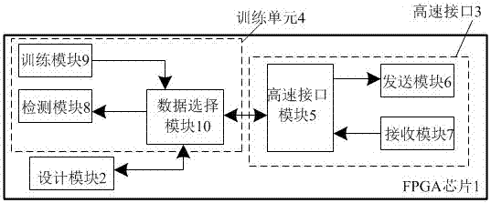
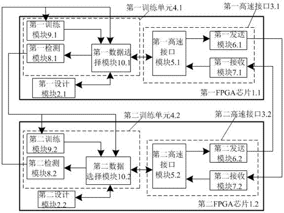
[0042] like figure 1 As shown, an FPGA chip provided in this embodiment includes a high-speed interface 3 and a training unit 4, the high-speed interface 3 includes a high-speed interface module 5, and the high-speed interface module 5 is connected with a sending module 6 and a receiving module 7;

[0043] The training unit 4 includes a data selection module 10 , the data selection module 10 is connected with the training module 9 and the detection module 8 ; the data selection module 10 is connected with the design module 2 ; the data selection module 10 is connected with the high-speed interface module 5 .

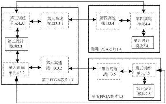
[0044] There are several high-speed interfaces 3 , and the number of training units 4 is the same as the number...


PUM


Abstract

The invention relates to an FPGA chip, a high-speed interface interconnection system and an interconnection achieving method. The FPGA chip is characterized by comprising an FPGA chip body, the FPGA chip body comprises a high-speed interface and a training unit, the high-speed interface comprises a high-speed interface module, and the high-speed interface module is connected with a transmitting module and a receiving module; the training unit comprises a data selection module, and the data selection module is connected with a training module and a detection module; the data selection module is connected with a design module; the data selection module is connected with the high-speed interface module; the FPGA chip body and the high-speed interface of at least another one FPGA chip. An automatic interconnection mechanism of the high-speed interface is put forwards, the high-speed interface interconnection success rate is increased, artificial participation is reduced, the debugging process is accelerated, and therefore the FPGA prototype verification period and the chip development period are greatly shortened.

Description

technical field [0001] The invention belongs to the technical field of FPGA prototype verification of server interconnection chips, and particularly relates to an FPGA chip, a high-speed interface interconnection system and a method for realizing interconnection. Background technique [0002] With the increasing number and complexity of business in daily life, the performance requirements for servers are also getting higher and higher. In order to provide server performance, improving the performance of a single CPU node can no longer satisfy people's expectations for server performance. Therefore, it is necessary to increase the number of CPU ways in the server to improve performance. [0003] The server interconnect chip (CC chip) is the core chip of the multi-processor shared main memory system. Its main function is to maintain global cache consistency, and realize global IO sharing and system-wide interruption. In order to make the system have good practical performance...

Claims


Application Information

Patent Timeline
IPC IPC(8): G06F17/50
CPCG06F30/30G06F30/367G06F2117/08
Inventor 周玉龙
Owner SUZHOU LANGCHAO INTELLIGENT TECH CO LTD
Why Eureka
Try Eureka