A load-balanced scanning forming method for a multi-laser SLM forming device

A load balancing and multi-laser technology, applied in the field of additive manufacturing, can solve problems such as uneven temperature field distribution, low working efficiency of the galvanometer group, and performance deterioration of the multi-laser overlapping area, achieving good bonding strength and ensuring maximum processing efficiency the effect of

Active Publication Date: 2019-03-05
HUAZHONG UNIV OF SCI & TECH
View PDF2 Cites 2 Cited by
  • Summary
  • Abstract
  • Description
  • Claims
  • Application Information

AI Technical Summary

Problems solved by technology

[0006] In view of the above deficiencies or improvement needs of the prior art, the present invention provides a load-balanced scanning forming method for a multi-laser SLM forming device, in which the geometric structure of the three-dimensional model and the performance and characteristics of the multi-laser galvanometer system are fully considered , to perform more optimized and effective segmentation of each discrete layer of the workpiece, and at the same time ensure that the workload of each laser galvanometer system on the discrete plane of the layer is basically the same; compared with the existing technology, it can effectively solve the problem of current multi-laser In the processing of SLM molding equipment, there are problems such as low working efficiency of the galvanometer group, uneven distribution of the temperature field, and performance deterioration in the multi-laser overlapping area. Large-scale workpiece manufacturing applications with internal structures

Method used


Image

  • A load-balanced scanning forming method for a multi-laser SLM forming device
  • A load-balanced scanning forming method for a multi-laser SLM forming device

Examples


Embodiment Construction

[0026] In order to make the object, technical solution and advantages of the present invention clearer, the present invention will be further described in detail below in conjunction with the accompanying drawings and embodiments. It should be understood that the specific embodiments described here are only used to explain the present invention, not to limit the present invention. In addition, the technical features involved in the various embodiments of the present invention described below can be combined with each other as long as they do not constitute a conflict with each other.

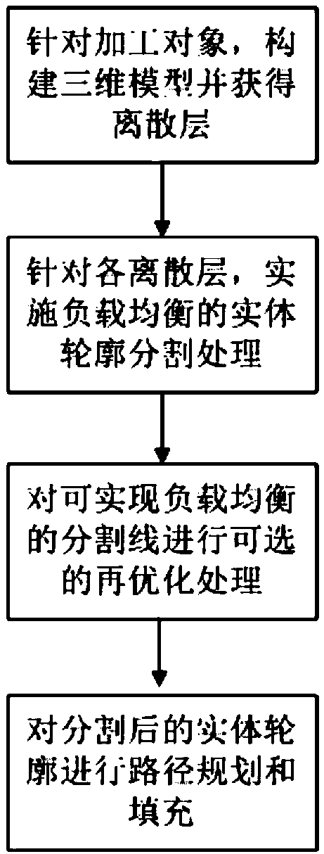
[0027] figure 1 It is a process flow diagram of a load-balanced scanning forming method for a multi-laser SLM forming device constructed according to the present invention. The following will refer to figure 1 , make specific explanations to the technical process and improvement points of the present invention.

[0028] First, there is the 3D modeling step.

[0029] Aiming at the parts to be...


PUM


Abstract

The invention belongs to the technical field related to additive manufacturing, and discloses a load-balanced scanning forming method for a multi-laser SLM forming device, including: (a) constructing a corresponding three-dimensional model for a component to be processed, and Perform layered slicing and discrete processing on the model, thereby obtaining the model profile of each discrete layer; (b) according to a certain algorithm, find the optimal dividing line in the middle overlapping area of ​​each two adjacent galvanometer scanning areas ; (c) implement path planning and filling for each area after the optimized segmentation, thereby completing the overall load balancing scanning forming process. The invention can effectively solve the problems of low working efficiency of the galvanometer group, uneven temperature field distribution, and performance deterioration of the multi-laser overlapping area existing in the processing of current multi-laser SLM forming equipment, and has high efficiency, high quality, and easy operation Features, so it is especially suitable for various large-scale workpiece manufacturing applications with complex internal structures.

Description

technical field [0001] The invention belongs to the technical field related to additive manufacturing, and more specifically relates to a load-balanced scanning forming method for a multi-laser SLM forming device. Background technique [0002] Selective Laser Melting (SLM) is a metal rapid prototyping method, which is based on the basic idea of ​​rapid prototyping "discrete-layer-by-layer", using metal powder as the processing raw material, according to the discrete three-dimensional model of each layer The shape of the slice is scanned and formed layer by layer by laser on the substrate with powder laid flat. During the forming process, the metal powder is completely melted under the action of the laser and then cooled to complete the metallurgical combination. Due to the advantages of short processing cycle, good forming quality, and the ability to process metal components with complex shapes, it has been widely used and developed in recent years. [0003] Selective lase...

Claims


Application Information

Patent Timeline
Patent Type & Authority Patents(China)
IPC IPC(8): B22F3/105B33Y10/00B33Y50/02
CPCB33Y10/00B33Y50/02B22F10/00B22F12/49B22F12/45B22F10/31B22F10/28Y02P10/25
Inventor 张李超何森赵祖烨史玉升
Owner HUAZHONG UNIV OF SCI & TECH
Why Eureka
Try Eureka