A mesa-type silicon-doped arsenic blocking impurity band detector and its preparation method

A technology for blocking impurities and detectors, applied in semiconductor devices, final product manufacturing, sustainable manufacturing/processing, etc., can solve the problem of long transmission path of photo-generated carriers, shortened transmission path of photo-generated carriers, and limited thickness of absorption layer To achieve the effect of improving absorption efficiency and device responsivity, shortening transport path, and reducing dark current

Active Publication Date: 2020-04-07
NO 50 RES INST OF CHINA ELECTRONICS TECH GRP
View PDF5 Cites 0 Cited by
  • Summary
  • Abstract
  • Description
  • Claims
  • Application Information

AI Technical Summary

Problems solved by technology

[0003] In view of the shortcomings of the above two silicon-based barrier impurity band detector preparation methods, the present invention uses chemical vapor deposition to epitaxially grow a silicon-doped arsenic absorber layer to solve the problem of the thickness of the absorber layer formed by ion implantation in a planar silicon-based barrier impurity band detector. It is convenient to increase the thickness of the absorbing layer and adjust the doping concentration, improve the absorption efficiency of the absorbing layer for very long-wave infrared radiation and the device responsivity, and at the same time avoid the damage caused by ion implantation and reduce the dark current; set the negative electrode at The upper surface of the high-conductivity silicon substrate solves the problem that the photo-generated carrier transmission path is long in the current mesa-type silicon-based barrier impurity band detector, so as to shorten the photo-generated carrier transmission path and reduce the recombination probability and Detector dark current, further improving the responsivity of the detector

Method used


Image

  • A mesa-type silicon-doped arsenic blocking impurity band detector and its preparation method
  • A mesa-type silicon-doped arsenic blocking impurity band detector and its preparation method
  • A mesa-type silicon-doped arsenic blocking impurity band detector and its preparation method

Examples


Embodiment 1

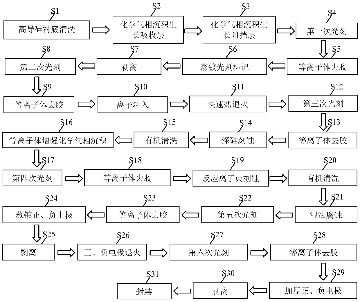
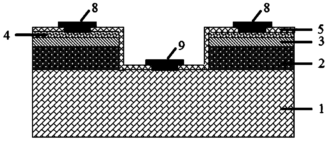
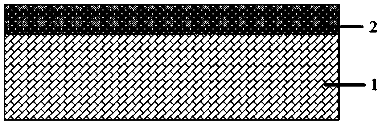
[0046] This embodiment relates to a mesa silicon arsenic-doped impurity barrier impurity band detector, which includes a high-conductivity silicon substrate 1 and a first region and a second region arranged on the high-conductivity silicon substrate 1; the first region includes sequential The silicon arsenic-doped absorption layer 2, the high-resistance silicon barrier layer 3, the positive electrode contact area 4 and the silicon nitride passivation layer 5 are provided, wherein the silicon-arsenic-doped absorption layer 2 is provided on the high-conductivity silicon substrate 1, The silicon nitride passivation layer 5 simultaneously covers the side surface composed of the silicon arsenic-doped absorption layer 2, the high-resistance silicon barrier layer 3 and the positive electrode contact area 4, and is provided on the silicon nitride passivation layer 5. There is a positive electrode 8; the second region includes a silicon nitride passivation layer 5 disposed on a high-cond...


PUM

PropertyMeasurementUnit
thicknessaaaaaaaaaa
thicknessaaaaaaaaaa
depthaaaaaaaaaa

Abstract

The invention provides a mesa type silicon-doped-arsenic blocked-impurity-band detector and a preparation method thereof. The preparation method comprises: carrying out epitaxial growth of a silicon-doped-arsenic absorption layer on a high-conductivity silicon substrate and carrying out doping of arsenic ions; carrying out epitaxial growth of high-resistance silicon barrier layer on the absorption layer; and carrying out photoetching, ion implantation, rapid thermal annealing, deep silicon etching, plasma-enhanced chemical vapor deposition, reactive ion beam etching, wet etching, electron beam evaporation and other processes to manufacture positive and negative electrodes. The detector and the preparation method have the following advantages: epitaxial growth of the silicon-doped-arsenic absorption layer is carried out by using a chemical vapor deposition method, so that the thickness of the absorption layer is increased and the doping concentration is adjusted, the absorption efficiency of the absorption layer and the device response ratio are improved, the damages caused by ion implantation are avoided, and the dark currents are reduced; and because the negative electrode is arranged on the high-conductivity silicon substrate, the transport path of the photo-generated carrier is shortened, the probability of photo-generated carrier capturing by impurities and defects in the high-conductivity silicon substrate is reduced, and thus the dark current of the device is reduced and the response rate is improved.

Description

Technical field [0001] The invention relates to the preparation process technology of a very long wave infrared (greater than 14 microns) detector, in particular to a method for manufacturing a mesa silicon-doped arsenic barrier impurity band detector, which is suitable for making mesa with low dark current and high response rate Type very long wave infrared blocking impurity band detector. Background technique [0002] The silicon-based barrier impurity band detector works in a low temperature environment below 10K, and can effectively detect very long-wave infrared radiation in the range of 14-40μm. It has broad application prospects in civil, military and aerospace fields. Currently, silicon-based barrier impurity band detectors mainly adopt the following two preparation methods: one is a planar (also called horizontal) structure preparation process, and the other is a mesa (also called vertical) structure preparation process. The planar structure preparation process is to f...

Claims


Application Information

Patent Timeline
Patent Type & Authority Patents(China)
IPC IPC(8): H01L31/09H01L31/0216H01L31/18C23C16/44
CPCC23C16/44H01L31/0216H01L31/09H01L31/1876Y02P70/50
Inventor 陈雨璐王兵兵王晓东张传胜谢巍侯丽伟潘鸣
Owner NO 50 RES INST OF CHINA ELECTRONICS TECH GRP
Why Eureka
Try Eureka