Organic electroluminescent diode, display substrate, methods for manufacturing same, and display device
A manufacturing method and display substrate technology, applied in the direction of organic semiconductor devices, circuits, electrical components, etc., can solve the problems of unfavorable display panel display effect, easy to cause microcavity effect, and unfavorable device performance, so as to improve the uniformity of light emission and prevent The effect of uneven light emission and elimination of viewing angle problems
- Summary
- Abstract
- Description
- Claims
- Application Information
AI Technical Summary
Problems solved by technology
Method used
Image
Examples
Embodiment 1
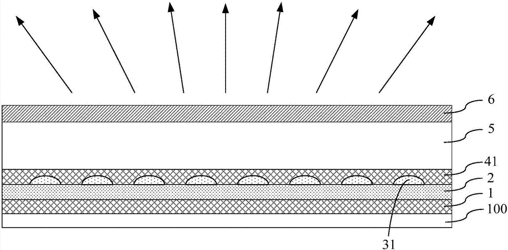
[0051] Such as figure 1 As shown, this embodiment provides an organic electroluminescent diode, including a first electrode and a second electrode 6 , and an organic light emitting layer 5 disposed between the first electrode and the second electrode 6 . The organic light emitting layer 5 is used to emit light of a specific color. The second electrode 6 is arranged close to the light emitting side of the organic electroluminescence diode. The first electrode includes a reflective conductive layer 2 , and the surface of the reflective conductive layer 2 close to the second electrode 6 has an uneven structure. figure 1The straight line with the arrow in the middle indicates the outgoing direction of the light emitted by the organic electroluminescence diode.
[0052] In the above technical solution, the first electrode of the organic electroluminescence diode includes a reflective conductive layer, and the surface of the reflective conductive layer close to the second electrod...
Embodiment 2
[0089] In this embodiment, a method for manufacturing the organic electroluminescent diode in Embodiment 1 is provided, and the method includes:
[0090] forming a first electrode and a second electrode, and the second electrode is disposed close to the light-emitting side of the organic electroluminescent diode;
[0091] An organic light emitting layer is formed between the first electrode and the second electrode.
[0092] see Figure 7 As shown, the step of forming the first electrode includes:
[0093] A reflective conductive layer is formed, and an uneven structure is formed on the surface of the reflective conductive layer close to the second electrode.
[0094] In the organic electroluminescent diode prepared by the above manufacturing method, the first electrode includes a reflective conductive layer, and an uneven structure is formed on the surface of the reflective conductive layer close to the second electrode. By forming the uneven structure, the first electrode ...
Embodiment 3
[0141] This embodiment provides a display substrate and a method for manufacturing the display substrate. The display substrate adopts the organic electroluminescence diode in the first embodiment. The manufacturing method of the display substrate includes the manufacturing method of the organic electroluminescent diode in the second embodiment. As for the specific structure and process steps of the display substrate, reference may be made to the prior art, which will not be described in detail here.
[0142] This embodiment also provides a display device, including the above-mentioned display substrate.
[0143] In the above technical solution, since the microcavity effect of the organic electroluminescent diode can be weakened or even eliminated, and the light scattering effect can be increased, the viewing angle problem of the display product can be eliminated and the display effect can be guaranteed.
[0144] The display device may be any product or component with a displ...
PUM
 Abstract
Description
Claims
Application Information


