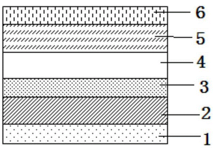
Top-emitting OLED device and preparation method thereof
A top-emitting device technology, applied in the field of lighting, can solve the problems of poor device efficiency, poor conductivity, high resistance, etc., and achieve the effect of eliminating plasma effect and viewing angle problem
- Summary
- Abstract
- Description
- Claims
- Application Information
AI Technical Summary
Problems solved by technology
Method used
Image
Examples
Embodiment 1
[0031] The OLED device structure and preparation method are specifically described below, wherein the structure of the OLED device is: glass substrate / Ag(150nm) / TiO 2 (800nm) / ITO(150nm) / NPB(40nm) / ADN:TBPe(7%)(30nm) / Alq 3 (20nm) / Mg:Ag(30%)(20nm) / Ag(10nm).
[0032] Its preparation method is specifically as follows:
[0033] (1) take the transparent glass as the substrate, and make a layer of 150nm Ag metal thereon as the reflective metal layer;
[0034] (2) Make a layer of scattering layer on the reflective metal layer, the thickness of the scattering layer is 800nm, wherein the process of making the scattering layer includes:
[0035] a) Dispersion process: put 15g of titanium dioxide, 1.2g of dispersant (afcma-4010), 60g of solvent (propylene glycol methyl ether acetate), and put the prepared solution into the grinding tank, fix the grinding tank and grinding column, add 90ml of zirconium beads (note: the amount of zirconium beads depends on the volume of the grinding tank)...
Embodiment 2
[0040] The structure of the OLED device is: glass substrate / Au(150nm) / SiO(3um) / IZO(1um) / NPB(40nm) / ADN:TBPe(7%)(30nm) / Alq 3 (20nm) / Mg:Ag(30%)(20nm) / Ag(10nm).
[0041] Its preparation method is specifically as follows:
[0042] (1) take transparent glass as the substrate, and make a layer of 150nm Au metal on it as the reflective metal layer;
[0043] (2) Fabricate a layer of silicon oxide scattering layer on the reflective metal layer. The thickness of the scattering layer is 3um. The manufacturing method is to spin-coat the silicon oxide dispersion liquid through a conventional photolithography process, and spin-coat to form a film.
[0044] (3) After the silicon oxide scattering layer is fabricated, a 1-micron IZO transparent electrode layer is prepared by a DC magnetron sputtering method. After the IZO transparent electrode layer is prepared, the IZO transparent electrode layer is etched by an etching method.
[0045] (4) Put the organic functional layer and the second ele...
Embodiment 3
[0047] The structure of the OLED device is: glass substrate / Pt(150nm) / ZrO 2 (300nm) / PEDOT:PSS(300nm) / NPB(40nm) / ADN:TBPe(7%)(30nm) / Alq 3 (20nm) / Mg:Ag(30%)(20nm) / Ag(10nm). Its preparation method is specifically as follows:
[0048] (1) take transparent glass as the substrate, and make a layer of 150nm Pt metal thereon as the reflective metal layer;
[0049] (2) Make a layer of ZrO on the reflective metal layer 2 The scattering layer, the thickness of the scattering layer is 300nm, is spin-coated by a conventional photolithography process, and spin-coated to form a film.
[0050] (3) ZrO 2 After the scattering layer is fabricated, a layer of PEDOT:PSS is spin-coated with a thickness of 300nm using a conventional photolithography process. After the transparent PEDOT:PSS electrode layer is prepared, the transparent electrode layer is etched out by an etching method.
[0051] (4) Put the organic functional layer and the second electrode layer into the evaporation chamber for e...
PUM
| Property | Measurement | Unit |
|---|---|---|
| thickness | aaaaa | aaaaa |
| thickness | aaaaa | aaaaa |
| thickness | aaaaa | aaaaa |
Abstract
Description
Claims
Application Information
