On-chip broadband coupling optical microcavity system and coupling method thereof

An optical microcavity and broadband technology, applied in the field of micro-nano optics, can solve the problem that waveguide mode and whispering gallery mode have different wave vector changes, cannot realize broadband coupling between optical waveguide and circular optical microcavity, and waveguide mode cannot be phase-matched, etc. problem, to achieve the effect of high measurement quality factor

Active Publication Date: 2017-12-22
PEKING UNIV
View PDF3 Cites 12 Cited by
  • Summary
  • Abstract
  • Description
  • Claims
  • Application Information

AI Technical Summary

Problems solved by technology

[0004] However, for different operating bands, the wave vector changes of the waveguide mode and the whispering gallery mode are not the same
Therefore, the waveguide mode in a single waveguide cannot be phase-matched with the whispering gallery mode in the microcavity in different optical bands, and the broadband coupling between the optical waveguide and the circular optical microcavity cannot be realized.

Method used


Image

  • On-chip broadband coupling optical microcavity system and coupling method thereof
  • On-chip broadband coupling optical microcavity system and coupling method thereof
  • On-chip broadband coupling optical microcavity system and coupling method thereof

Examples


Embodiment 1

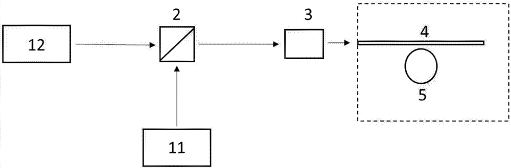
[0026] like figure 2 As shown, the on-chip integrated broadband coupling optical microcavity system of this embodiment includes: a first laser light source 11, a second laser light source 12, a beam combining mirror 2, a focusing objective lens 3, an optical waveguide 4, and a non-circular optical microcavity 5 and a chip; the optical waveguide 4 and the non-circular optical microcavity are integrated in the chip.

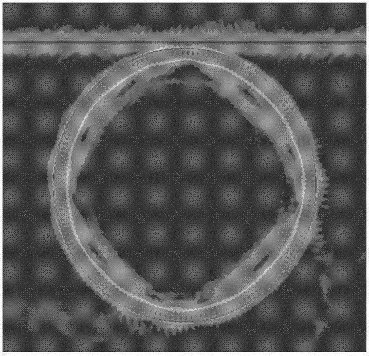
[0027] In this embodiment, the optical waveguide has a width of 500 nanometers and a thickness of 500 nanometers. The boundary equation of the non-circular optical microcavity is where n=4, R 0 = 50 microns, a 1 = 0.031644, a 2 =-0.099768,a 3 = 0.012216, a 4 =0.012828, η=18% The optical waveguide and the non-circular optical microcavity adopt silicon dioxide.

[0028] The output laser wavelength of the first laser light source 11 is 1550 nanometers, and the output laser wavelength of the second laser light source 12 is 780 nanometers. The output laser ligh...

Embodiment 2

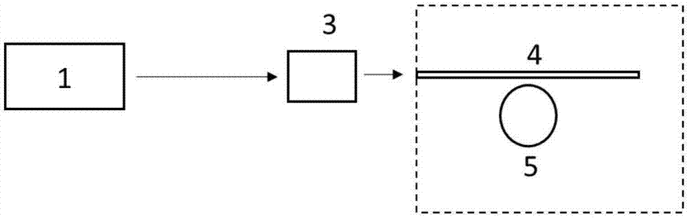
[0031] like image 3 As shown, the on-chip integrated broadband coupling optical microcavity system of this embodiment includes: a laser light source 1 , a focusing objective lens 3 , an optical waveguide 4 and a non-circular optical microcavity 5 .

[0032] In this embodiment, the optical waveguide has a width of 500 nanometers and a thickness of 500 nanometers. The boundary equation of the non-circular optical microcavity is where n=4, R 0 = 50 microns, a 1 = 0.031644, a 2 =-0.099768, a 3 = 0.012216, a 4 = 0.012828, η = 18%. The optical waveguide and non-circular optical microcavity adopt lithium niobate.

[0033] The laser light source 1 outputs a laser with a wavelength of 1550 nanometers. The focusing objective lens 3 focuses on the end face of the optical waveguide 4, and then couples from the optical waveguide 4 to the non-circular optical microcavity 5. The interaction between light and matter is enhanced through the optical microcavity. The second harmonic is...


PUM


Abstract

The present invention discloses an on-chip broadband coupling optical microcavity system and a coupling method thereof. In the invention, a non-circular optical microcavity and an optical waveguide prepared on a chip are adopted, and the slight deformation of the non-circular optical microcavity causes the eigenstate echo wall mode originally distributed only in the edge of the circular optical microcavity to extend into the non-circular optical microcavity, forming a "tail"; laser and the "tail" of the non-circular optical microcavity are in phase matching, so as to stimulate the excited state echo wall mode of the non-circular optical microcavity; the echo wall mode of the non-circular optical microcavity can be refracted into the optical waveguide through its "tail"; the optical waveguide enables effective broadband excitation and collection of the echo wall mode in the non-circular optical microcavity, i.e., the completion of the effective broadband coupling of the optical waveguide and the non-circular optical microcavity; and the deformation of the non-circular optical microcavity is so little that the non-circular optical microcavity can maintain high intrinsic quality factors (> 10<4>) without introducing large radiation losses.

Description

technical field [0001] The invention relates to micro-nano optics, in particular to an on-chip integrated broadband coupling optical microcavity system and a coupling method thereof. Background technique [0002] Optical microcavities can store optical energy for a long time in a small volume, greatly enhancing the interaction between light and matter. The total internal reflection of the surface of the medium occurs when the light from the high refractive index (n 1 ) materials towards low refractive index (n 0 ) when the material is incident, and the incident angle satisfies θ≥arcsin(n 0 / n 1 ). Considering that a beam of light propagates in a disk cavity through continuous reflection at the boundary, the rotational symmetry of the circle will ensure that the incident angle of the light remains constant, and the total reflection condition will always be satisfied. The phase delay of the light moving along the boundary for one week must be equal to 2πm (m=1,2,3...), so...

Claims


Application Information

Patent Timeline
Patent Type & Authority Applications(China)
IPC IPC(8): H01S5/00
CPCH01S5/005
Inventor 肖云峰姜雪峰邵林博张树昕王栗龚旗煌
Owner PEKING UNIV
Why Eureka
Try Eureka