

A kind of ldmos device with stepped trench
A stepped, trench technology, applied in semiconductor devices, electrical components, circuits, etc., can solve the problems of substrate depletion, substrate-assisted depletion, inability to optimize the electric field in the drift region, etc., and achieve vertical electric field distribution. Uniform and improve the effect of reverse blocking voltage
- Summary
- Abstract
- Description
- Claims
- Application Information
AI Technical Summary
Problems solved by technology
Method used
Image

Examples
Embodiment Construction
[0014] Embodiments of the present invention are described below through specific examples, and those skilled in the art can easily understand other advantages and effects of the present invention from the content disclosed in this specification. The present invention can also be implemented or applied through other different specific implementation modes, and various modifications or changes can be made to the details in this specification based on different viewpoints and applications without departing from the spirit of the present invention.
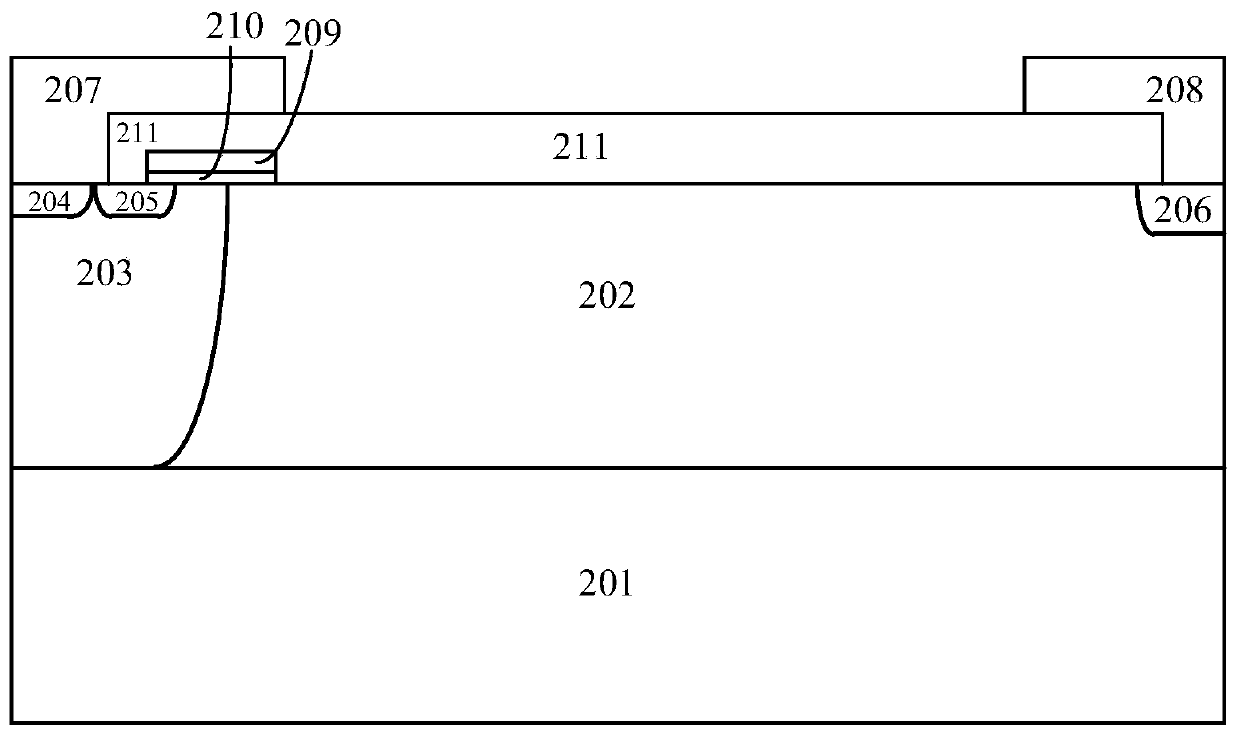
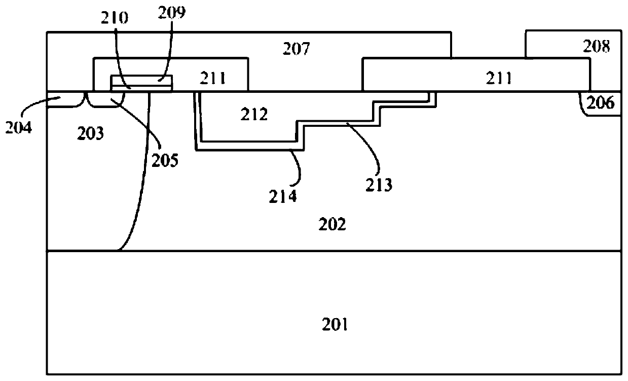
[0015] Such as figure 2 As shown, an LDMOS device with stepped trenches includes a first conductivity type semiconductor substrate 201 and a first conductivity type semiconductor body region 203 and a second conductivity type semiconductor body region 203 disposed on the upper surface of the first conductivity type semiconductor substrate 201 The semiconductor drift region 202, the first conductivity type semiconductor body region 20...
PUM
 Abstract
Description
Claims
Application Information