Metal oxide diode with high voltage withstanding and low conduction voltage drop characteristics

A technology of conduction voltage drop and oxide, which is applied in the direction of semiconductor devices, electrical components, circuits, etc., can solve the problems of low forward conduction voltage drop and high forward conduction voltage drop, and achieve low conduction voltage drop and conduction The effect of reducing the voltage drop and increasing the reverse blocking voltage

Inactive Publication Date: 2016-09-21
UNIV OF ELECTRONICS SCI & TECH OF CHINA
View PDF5 Cites 0 Cited by
  • Summary
  • Abstract
  • Description
  • Claims
  • Application Information

AI Technical Summary

Problems solved by technology

[0004] The purpose of the present invention is to solve the problem of high forward conduction voltage drop of shallow groove metal oxide diodes in the medium and high voltage field, so that the device can achieve low forward conduction voltage drop while ensuring a high reverse withstand voltage

Method used


Image

  • Metal oxide diode with high voltage withstanding and low conduction voltage drop characteristics
  • Metal oxide diode with high voltage withstanding and low conduction voltage drop characteristics
  • Metal oxide diode with high voltage withstanding and low conduction voltage drop characteristics

Examples


Embodiment 1

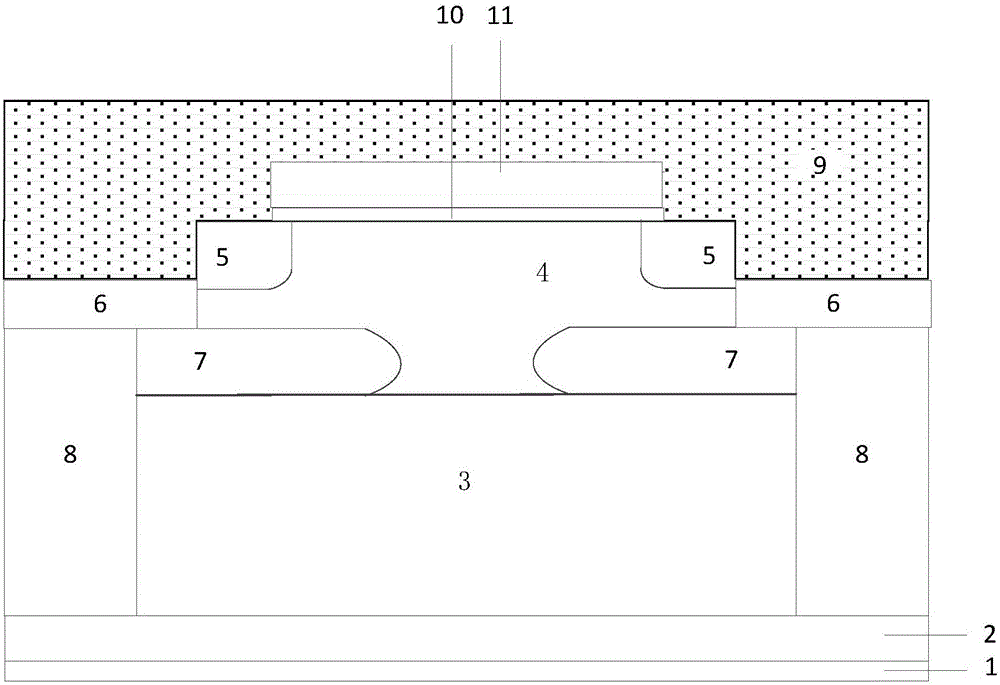
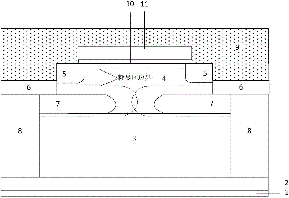
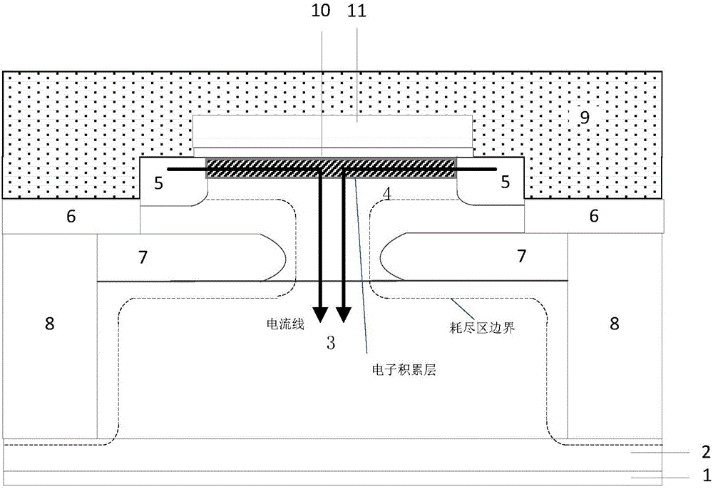
[0023] Such as figure 1 As shown, the metal oxide diode with high withstand voltage and low conduction voltage drop characteristics in this example includes an anode electrode 9, an N-doped region 4, an N-type region 3, an N-type heavy Doped monocrystalline silicon substrate 2 and cathode electrode 1; the two ends of the anode electrode 9 extend vertically downward into the N-doped region 4, and the part between the N-doped region 4 and the downwardly extending part of the anode electrode 9 There is an N-type heavily doped region 5 between them; the upper surface of the N-doped region 4 between the N-type heavily doped regions 5 on both sides has a planar gate structure, and the planar gate structure is located in the anode electrode 1, and the plane The gate structure includes a gate oxide layer 10 and a polysilicon gate electrode 11 located on the upper surface of the oxide layer 10, the lower surface of the oxide layer 10 is in contact with the upper surface of part of the ...

Embodiment 2

[0034] Such as Image 6 As shown, the structure of this example is based on Example 1, the thickness of the N-type region 3 is reduced, the thickness of the N-doped region 4 is increased, and extends to the bottom of the P-type region 7, the working principle of this example Similar to Embodiment 1, the turn-on voltage can be further lowered.

Embodiment 3

[0036] Such as Figure 7 As shown, the structure of this example is based on Embodiment 1, and a layer of N-type epitaxial layer 12 is grown on an N-type heavily doped single crystal silicon substrate, and the concentration of N-type epitaxial layer 12 is related to the concentration of N-type drift region 3 The concentrations are different, and the thicknesses of the N-type region 3 and the P-type region 8 are simultaneously reduced. In order to meet different requirements, the concentration of the N-type epitaxial layer 12 can be adjusted. In order to further reduce the turn-on voltage drop, the doping concentration of the N-type epitaxial layer 12 can be increased; in order to increase the reverse withstand voltage, the doping concentration of the N-type epitaxial layer 12 can be decreased.


PUM


Abstract

The invention relates to the semiconductor technology and particularly relates to a metal oxide semiconductor diode with high voltage withstanding and low conduction voltage drop characteristics. The metal oxide semiconductor diode comprises an electron accumulation layer structure and a junction field effect transistor structure and can obtain low conduction voltage drop. At the same time, an N type area 3 with a high doping concentration is employed, and the conduction voltage drop of the diode in positive conduction is reduced further. When a device is reversely blocked, the acceptor impurities contained in a P type area 8 and a P type buried layer 8 and the donor impurity contained in the N type area are mutually depleted, thus the electric field distribution of a drift area is in a rectangular distribution, and the reverse blocking voltage of the device can be raised. Therefore, the new structure of the invention has the advantages of high voltage withstanding and low conduction voltage drop.

Description

technical field [0001] The invention relates to semiconductor technology, in particular to a metal oxide diode with high withstand voltage and low turn-on voltage drop characteristics. Background technique [0002] Diodes are one of the most commonly used electronic components. Traditional rectifier diodes are mainly Schottky rectifiers and PN junction rectifiers. Among them, the PN junction diode can withstand a high reverse blocking voltage and has good stability, but its forward conduction voltage drop is relatively large, and its reverse recovery time is relatively long. Schottky diodes are manufactured using the principle of metal-semiconductor junctions formed by metal-semiconductor contacts, and the on-state voltage drop is low. Due to the conduction of unipolar carriers, Schottky diodes have no excess minority carrier accumulation during forward conduction, and the reverse recovery is relatively fast. However, the reverse breakdown voltage of the Schottky diode is ...

Claims


Application Information

Patent Timeline
Patent Type & Authority Applications(China)
IPC IPC(8): H01L29/861H01L29/06
CPCH01L29/8613H01L29/0607H01L29/0692
Inventor 任敏李爽陈哲曹晓峰李泽宏张金平高巍张波
Owner UNIV OF ELECTRONICS SCI & TECH OF CHINA
Why Eureka
Try Eureka