

SiC crystal and semiconductor device
a semiconductor and crystal technology, applied in the direction of soldering apparatus, manufacturing tools, capacitors, etc., can solve the problems of low conversion efficiency of red phosphors, inferior color rendering as illumination light source, and inadequate energy conversion efficiency of the above-described white light light-emitting diodes compared with existing fluorescent lamps
- Summary
- Abstract
- Description
- Claims
- Application Information
AI Technical Summary
Benefits of technology
Problems solved by technology
Method used
Image

Examples
Embodiment Construction
[0019]The detailed description set forth below in connection with the appended drawings is intended as a description of presently preferred embodiments of the invention and is not intended to represent the only forms in which the present invention may be constructed and or utilized.
[0020]Here, aspects of the invention are explained, according to the following order.
[0021]A. Structure, method of fabrication, and applications of SiC phosphors
[0022]B. Impurity concentration settings
[0023]C. Modified example of SiC phosphors
[0024]D. Structure, method of fabrication, and applications of white-light light-emitting diode
[0025]E. Summary
A. Structure, Method of Fabrication, and Applications of SiC Phosphors
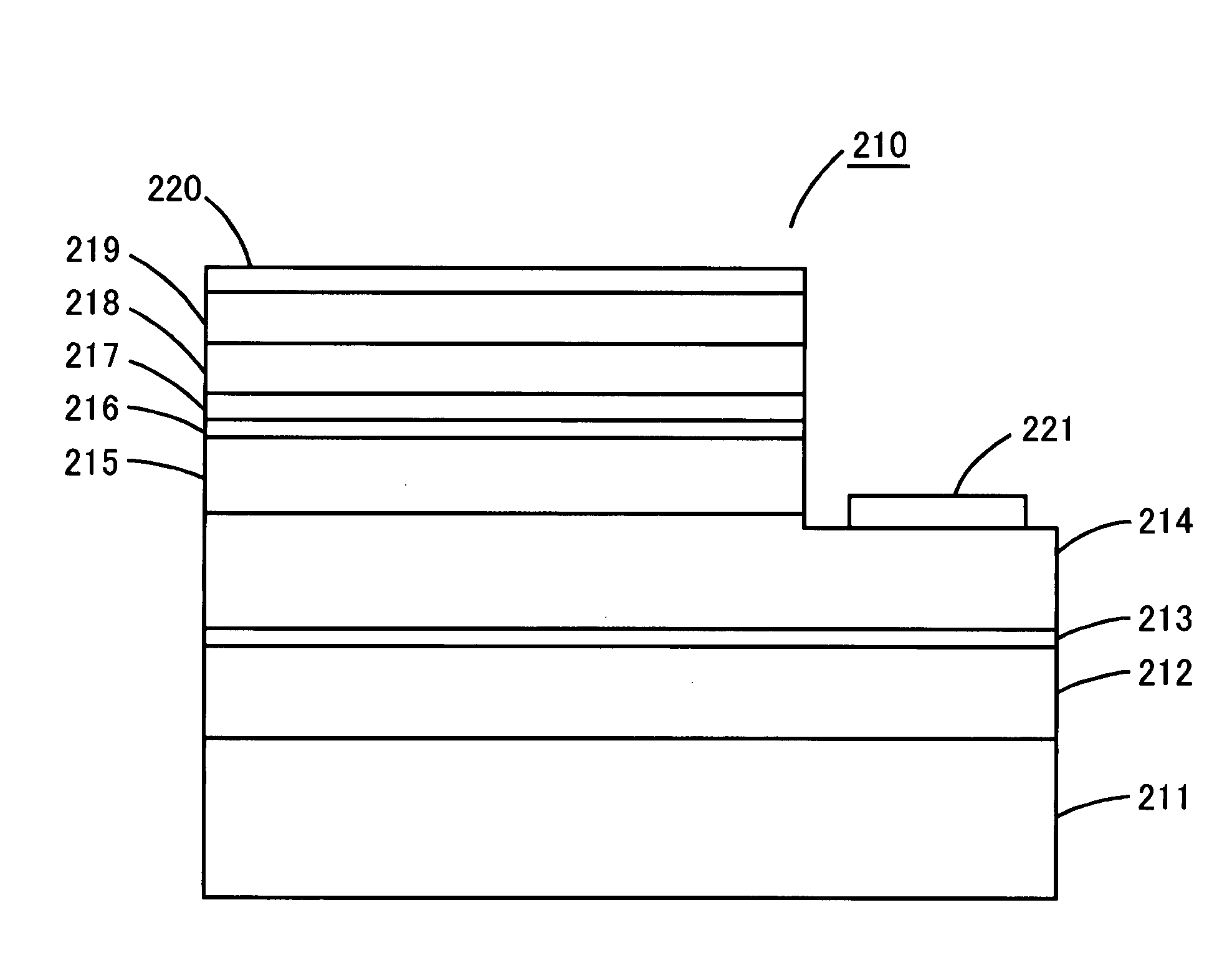
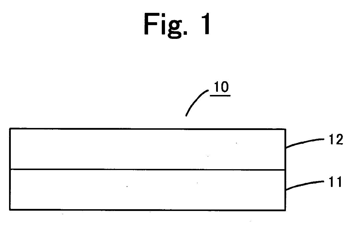
[0026]FIG. 1 schematically shows the structure of SiC phosphors as SiC crystals in one aspect. In the drawing, the SiC phosphor 10 comprises a SiC substrate 11 and a SiC fluorescent layer 12. The SiC substrate 11 is formed using a 6H-type SiC crystal, having a periodic structure repeating ...
PUM
| Property | Measurement | Unit |
|---|---|---|
| thickness | aaaaa | aaaaa |
| fluorescent light quantum efficiency | aaaaa | aaaaa |
| fluorescent light quantum efficiency | aaaaa | aaaaa |
Abstract
Description
Claims
Application Information