Preparation method of enhanced high-electron-mobility transistor

A high electron mobility, transistor technology, applied in semiconductor/solid-state device manufacturing, circuits, electrical components, etc., can solve the problem of low carrier concentration in the p-type layer, achieve weakening passivation effect, and increase carrier concentration , the effect of increasing the ionization rate

Active Publication Date: 2018-08-24
THE 13TH RES INST OF CHINA ELECTRONICS TECH GRP CORP
View PDF3 Cites 5 Cited by
  • Summary
  • Abstract
  • Description
  • Claims
  • Application Information

AI Technical Summary

Problems solved by technology

[0004] In view of this, an embodiment of the present invention provides a method for manufacturing an enhanced high

Method used


Image

  • Preparation method of enhanced high-electron-mobility transistor
  • Preparation method of enhanced high-electron-mobility transistor

Examples


Embodiment 1

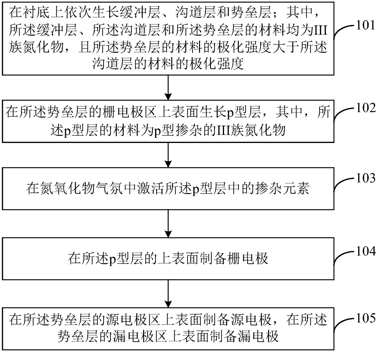
[0031] Please refer to figure 1 , a method for preparing an enhanced high electron mobility transistor, comprising:

[0032] Step S101, sequentially growing a buffer layer, a channel layer, and a barrier layer on a substrate; wherein, the materials of the buffer layer, the channel layer, and the barrier layer are all Group III nitrides, and the The polarization of the material of the barrier layer is greater than the polarization of the material of the channel layer.

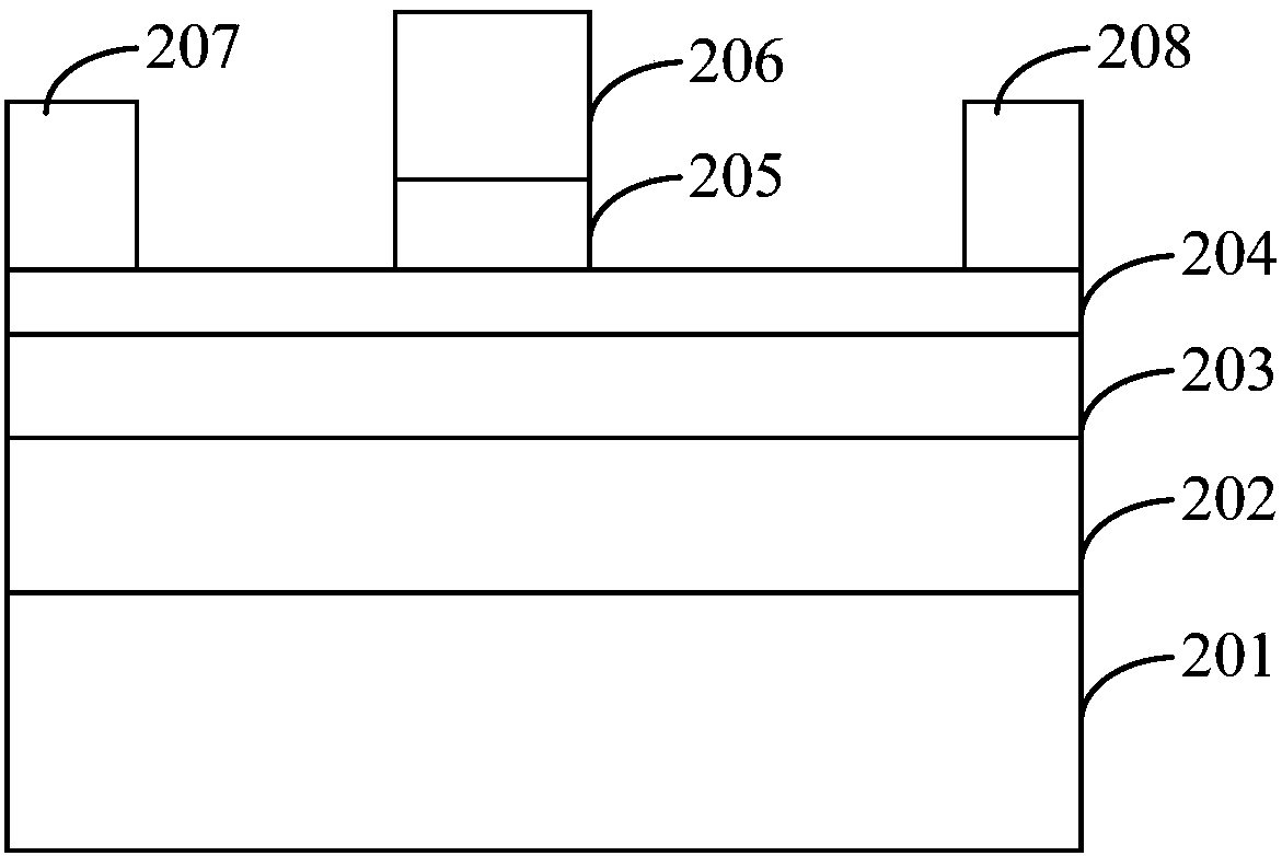
[0033] In the embodiment of the present invention, please refer to figure 2 , epitaxially epitaxially group III nitride buffer layer 202 , group III nitride channel layer 203 and group III nitride barrier layer 204 on the substrate 201 by an epitaxial process. Epitaxial processes include, but are not limited to, metal organic chemical vapor deposition, molecular beam epitaxy deposition, pulsed laser deposition, magnetron sputtering deposition, electron beam evaporation deposition, and chemical vapor depositio...

Embodiment 2

[0058] The preparation method of the enhanced high electron mobility transistor includes: first, a 1.5 μm GaN buffer layer, a 200 nm GaN channel layer, and a 20 nm Al 0.2 Ga 0.8 N barrier layer and 200nm GaN p-type layer, wherein the doping element in the p-type layer is Mg, and the doping concentration is 10 18 cm -3 , and then, put the substrate after growing the p-type layer into the magnetron sputtering chamber, and evacuate to 10 -6 mbar, N is passed into the magnetron sputtering chamber 2 O and O 2 , where N 2 The volume fraction of O is 40%, O 2 The volume fraction is 60%, the chamber pressure is controlled at 1mbar, and the atmosphere is stabilized for 2 minutes. After the atmosphere is stabilized, the magnetron sputtering power is set to 1W, and the Mg-doped p-type layer is plasma treated at room temperature. The processing time is 10s, and then use the photolithography process and the electron beam evaporation process to evaporate Ni / Au on the upper surface of ...


PUM

PropertyMeasurementUnit
Thicknessaaaaaaaaaa
Thicknessaaaaaaaaaa
Thicknessaaaaaaaaaa

Abstract

The invention is suitable for the technical field of semiconductors, and provides a preparation method of an enhanced high-electron-mobility transistor. The method comprises the steps that a buffer layer, a channel layer and a barrier layer are grown on a substrate in turn, wherein the material of the buffer layer, the channel layer and the barrier layer is the III-nitride, and the intensity of polarization of the material of the barrier layer is greater than that of the material of the channel layer; a p-type doped III-nitride p-type layer is grown on the upper surface of the gate electrode region of the barrier layer; the doping element in the p-type layer is activated in the atmosphere of the nitrogen oxide; a gate electrode is formed on the upper surface of the p-type layer; and a source electrode is formed on the upper surface of the source electrode region of the barrier layer, and a drain electrode is formed on the upper surface of the drain electrode region of the barrier layer. The ionization rate of the acceptor impurities can be enhanced and thus the carrier concentration of the p-type layer can be enhanced.

Description

technical field [0001] The invention belongs to the technical field of semiconductors, in particular to a preparation method of an enhanced high electron mobility transistor. Background technique [0002] A high electron mobility transistor (High Electron Mobility Transistor, HEMT) is a heterojunction field effect transistor. The high-mobility two-dimensional electron gas exists in the heterojunction, which makes HEMT devices have high frequency, high power, and high temperature resistance. and excellent properties such as radiation resistance. At present, most HEMT devices based on III-nitride materials are depletion-mode devices, which must be biased with a negative voltage on the gate when they are turned off, which increases the power consumption and complexity of the circuit, and reduces the system performance. safety. Enhanced HEMT devices can reduce system power consumption and complexity, improve security, and have broad application prospects in high-temperature an...

Claims


Application Information

Patent Timeline
IPC IPC(8): H01L21/335
CPCH01L29/66431
Inventor 房玉龙郭艳敏尹甲运李佳张志荣王波芦伟立高楠冯志红
Owner THE 13TH RES INST OF CHINA ELECTRONICS TECH GRP CORP
Why Eureka
Try Eureka