Silicon infrared optical detector structure and manufacturing method therefor

A manufacturing method and photodetector technology, applied in photovoltaic power generation, semiconductor devices, final product manufacturing, etc., can solve the problems of shortening the lifetime of non-equilibrium carriers, not easy to ionize, and difficult to control the energy level

Inactive Publication Date: 2016-09-07
NAT CENT FOR ADVANCED PACKAGING
View PDF3 Cites 6 Cited by
  • Summary
  • Abstract
  • Description
  • Claims
  • Application Information

AI Technical Summary

Problems solved by technology

[0004] In view of the above-mentioned and/or existing problems in existing silicon devices such as the use of deep-level impurity doping that is not

Method used


Image

  • Silicon infrared optical detector structure and manufacturing method therefor
  • Silicon infrared optical detector structure and manufacturing method therefor
  • Silicon infrared optical detector structure and manufacturing method therefor

Examples


Embodiment 1

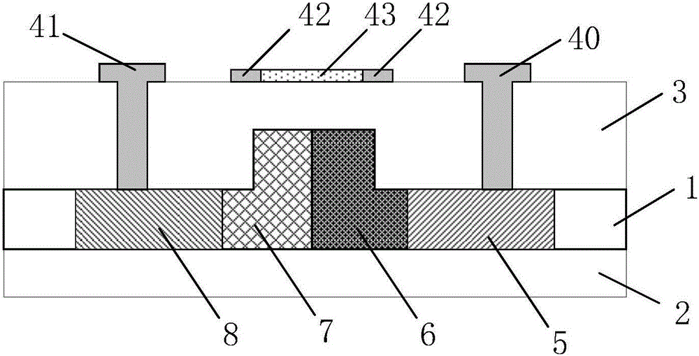
[0055] Such as figure 1 Shown: the structure of the silicon infrared photodetector of the present invention comprises a dielectric layer 2, a single crystal silicon layer 1 and a passivation layer 3 arranged in sequence from bottom to top, and a resistance heater is arranged on the surface of the passivation layer 3, and the resistance heating The device includes the electrode 42 of the resistance heater and the resistance part 43 of the resistance heater; the upper surface of the single crystal silicon layer 1 is etched to form a ridge-shaped optical waveguide, and the single crystal silicon layer 1 is provided with a re-donor compensation Superheavy acceptor doped region (P ++ N +) 7, superheavy donor doped region with heavy acceptor compensation (N++P+) 6, superheavy acceptor doped region (P++) 8 and superheavy donor doped Region (N++) 5, superheavy acceptor doped region (P ++ N + ) 7 with heavy donor compensation and superheavy donor doped region (N++P+) 6 with heavy accep...

Embodiment 2

[0075] Such as Figure 15 Shown: the structure of the silicon infrared photodetector of the present invention includes a single crystal silicon substrate 10, and the upper surface of the single crystal silicon substrate 10 is etched to form a ridge-shaped optical waveguide; on the single crystal silicon substrate 10 The upper surface is covered with a passivation layer 3, and the passivation layer 3 evenly covers the ridge optical waveguide and the two wings of the ridge optical waveguide; in the single crystal silicon substrate 10, a superheavy acceptor doped region ( P ++ N +) 7, super heavy donor doped region with heavy acceptor compensation (N++P+) 6, super heavy acceptor doped region (P++) 8, super heavy donor doped region (N ++) 5 and heavy Acceptor doped region (P+)9, superheavy acceptor doped region with heavy donor compensation (P++N+)7 and superheavy donor doped region with heavy acceptor compensation (N++P+)6 Arranged along the side walls and top of the ridge optic...

Embodiment 3

[0084] Such as Figure 21Shown: the structure of the silicon infrared detector of the present invention, including a dielectric layer 2, a single crystal silicon layer 1 and a passivation layer 3 arranged in sequence from bottom to top, and the upper surface of the single crystal silicon layer 1 is etched to form a ridge Shaped optical waveguide, the superheavy acceptor doped region (P ++ N + ) 7, the superheavy acceptor doped region (P++) 8 and the heavy donor doped region ( N+) 15, superheavy acceptor doped region (P++ N+) 7 with heavy donor compensation located in the region of the ridge optical waveguide, superheavy acceptor doped region (P++) 8 and heavy donor doped region (N+ ) 15 are located on the two wings of the ridge optical waveguide; the upper surface of the passivation layer 3 is close to a plane, and an N-type electrode 40 and a P-type electrode 41 are arranged in the passivation layer 3, the N-type electrode 40 is the cathode of the detector, and the P The N-t...


PUM

PropertyMeasurementUnit
Thicknessaaaaaaaaaa
Carrier concentrationaaaaaaaaaa

Abstract

The invention relates to a silicon infrared optical detector structure and a manufacturing method therefor. A super-heavy doped silicon single crystal material with weight compensation is taken as an infrared photoelectric conversion material; a super-heavy donor doped silicon single crystal material with weight acceptor compensation or a super-heavy acceptor doped silicon single crystal material with weight donor compensation is singly adopted for absorbing infrared light to generate electron-hole pairs; or the super-heavy donor doped silicon single crystal material with weight acceptor compensation and the super-heavy acceptor doped silicon single crystal material with weight donor compensation are adopted concurrently to form a PN junction for absorbing infrared light to generate the electron-hole pairs. According to the silicon infrared optical detector structure, the donor impurity and the acceptor impurity are heavily doped in the silicon single crystal material concurrently, so that a donor impurity energy band and an acceptor impurity energy band are formed in a forbidden band at the same time; meanwhile, an energy band tail connected with a conduction band and an energy band tail connected with a valence band are formed as well, so that the energy levels of the impurities participate in the infrared photon absorption and electron and hole jumps; and therefore, the photoelectric conversion efficiency of the silicon material at the near infrared communication waveband is improved.

Description

technical field [0001] The invention relates to a structure of a silicon infrared photodetector and a manufacturing method thereof, belonging to the technical field of silicon-based photoelectric integration. Background technique [0002] The forbidden band width of silicon is about 1.12ev, and the spectral absorption limit of intrinsic light absorption is at 1110nm. At present, the optical windows of optical communication are in the infrared bands such as 1310nm, 1490nm, and 1550nm, so the photodetectors working in these infrared bands are currently mainly made of III-V materials. Silicon is the most widely used semiconductor material with the most mature technology and the most complete industry. Silicon has an unrivaled position in the field of electronics, and the demand for the fusion of light and electricity makes silicon photonics technology a research hotspot. In addition to the intrinsic light absorption of semiconductor materials, silicon also has extrinsic light...

Claims


Application Information

Patent Timeline
IPC IPC(8): H01L31/0216H01L31/0352H01L31/18
CPCH01L31/02161H01L31/03529H01L31/1868Y02E10/50Y02P70/50
Inventor 李宝霞薛海韵
Owner NAT CENT FOR ADVANCED PACKAGING
Why Eureka
Try Eureka