Low divergence angle full Bragg reflector waveguide semiconductor laser array

A Bragg reflection and laser array technology, applied in the structure of optical waveguide semiconductors, etc., can solve the problems of poor beam quality, complex process, large divergence angle, etc., to reduce the longitudinal and lateral divergence angles, mature preparation process, and good repeatability Effect

Active Publication Date: 2012-07-25
CHANGCHUN INST OF OPTICS FINE MECHANICS & PHYSICS CHINESE ACAD OF SCI
View PDF7 Cites 13 Cited by
  • Summary
  • Abstract
  • Description
  • Claims
  • Application Information

AI Technical Summary

Problems solved by technology

The bottleneck of achieving high brightness is mainly the problem of poor beam quality. Traditional edge-emitting semiconductor lasers have a large divergence angle, which is 45° in the longitudinal direction (fast axis) and 10° in the lateral direction (slow axis).
Although the divergence angle of semiconductor lasers can be compressed to a certain extent by beam shaping, the process is complicated and the cost is high

Method used


Image

  • Low divergence angle full Bragg reflector waveguide semiconductor laser array
  • Low divergence angle full Bragg reflector waveguide semiconductor laser array
  • Low divergence angle full Bragg reflector waveguide semiconductor laser array

Examples


Embodiment Construction

[0012] The present invention will be further described in detail below in conjunction with the accompanying drawings and specific embodiments.

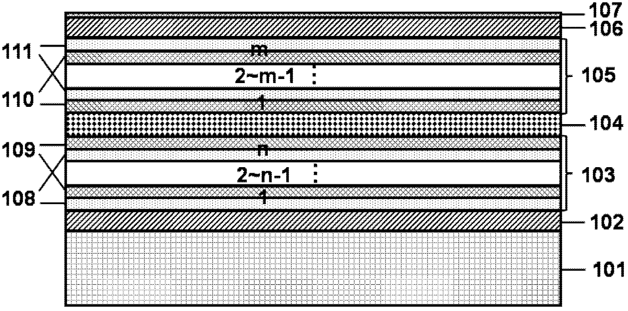
[0013] Such as figure 1 As shown, the longitudinal structure of the low divergence angle full Bragg reflective waveguide semiconductor laser array of the present invention is as follows from bottom to top: N-type substrate 101, N-type confinement layer 102, N-type Bragg reflective waveguide 103, active region 104, P-type Bragg reflection waveguide 105 , P-type confinement layer 106 , and P-type capping layer 107 . Among them, the N-type Bragg reflective waveguide 103 is composed of n (n≥1) pairs of high and low refractive index materials periodically arranged, and each period includes an N-type high-refractive-index layer 108 and an N-type low-refractive-index layer 109; a P-type Bragg The reflective waveguide 105 is composed of m (m≥1) pairs of high and low refractive index materials periodically arranged, and each period includes a...


PUM


Abstract

The invention relates to a low divergence angle full Bragg reflector waveguide semiconductor laser array, belonging to the field of the semiconductor laser. For lowering the longitudinal and transverse divergence angle, improving the beam quality of the laser and obtaining the high luminance laser output, the invention designs the low divergence angle full Bragg reflector waveguide semiconductor laser array. The array longitudinal structure comprises an N-type substrate, an N-type limiting layer, an N-type Bragg reflector waveguide, an active area, a P-type Bragg reflector waveguide, a P-type limiting layer and a P-type cap layer in turn from bottom to top. The N-type Bragg reflector waveguide and P-type Bragg reflector waveguide in the longitudinal structure are formed by respectively arranging at least one pair of high and low refractive index materials periodically. The array transverse structure comprises a current injection area and a transverse Bragg reflector waveguide set at two sides thereof. The transverse Bragg reflector waveguide set at two sides are respectively formed by arranging at least one pair of high and low ridge structures periodically. The lower ridge part is close to the current injection area. The low divergence angle full Bragg reflector waveguide semiconductor laser array realizes the high luminance laser output.

Description

technical field [0001] The invention relates to the field of semiconductor lasers, in particular to a low divergence angle full Bragg reflective waveguide semiconductor laser array. Background technique [0002] High-brightness semiconductor lasers have the advantages of high power and high beam quality, and have important applications in the fields of communication, medical treatment, material processing, pumping solid-state lasers and fiber lasers. At present, great progress has been made in the development of high-power semiconductor lasers, and the output power of a single-tube device can reach the order of hundreds of watts. The bottleneck of achieving high brightness is mainly the problem of poor beam quality. Traditional edge-emitting semiconductor lasers have a large divergence angle, which is 45° in the longitudinal direction (fast axis) and 10° in the lateral direction (slow axis). Although the divergence angle of the semiconductor laser can be compressed to a cer...

Claims


Application Information

Patent Timeline
Patent Type & Authority Applications(China)
IPC IPC(8): H01S5/22
Inventor 杨晔佟存柱汪丽杰王立军曾玉刚刘云
Owner CHANGCHUN INST OF OPTICS FINE MECHANICS & PHYSICS CHINESE ACAD OF SCI
Why Eureka
Try Eureka