ESD protection integrated power MOSFET or IGBT and preparation method thereof

An ESD protection and power technology, which is applied in semiconductor/solid-state device manufacturing, electrical components, electric solid-state devices, etc., can solve problems such as complex circuits, increased manufacturing costs, and large area occupied by ESD protection, achieving good universality, The effect of cost reduction and improvement of ESD discharge capability

Active Publication Date: 2011-03-02
江苏东晨电子科技有限公司 +1
View PDF2 Cites 14 Cited by
  • Summary
  • Abstract
  • Description
  • Claims
  • Application Information

AI Technical Summary

Problems solved by technology

However, it adopts the combination structure of the primary branch and the secondary branch, which makes the circuit complex; and the ESD protection occupies a large area, which increases the manufacturing cost

Method used


Image

  • ESD protection integrated power MOSFET or IGBT and preparation method thereof
  • ESD protection integrated power MOSFET or IGBT and preparation method thereof
  • ESD protection integrated power MOSFET or IGBT and preparation method thereof

Examples


Embodiment 1

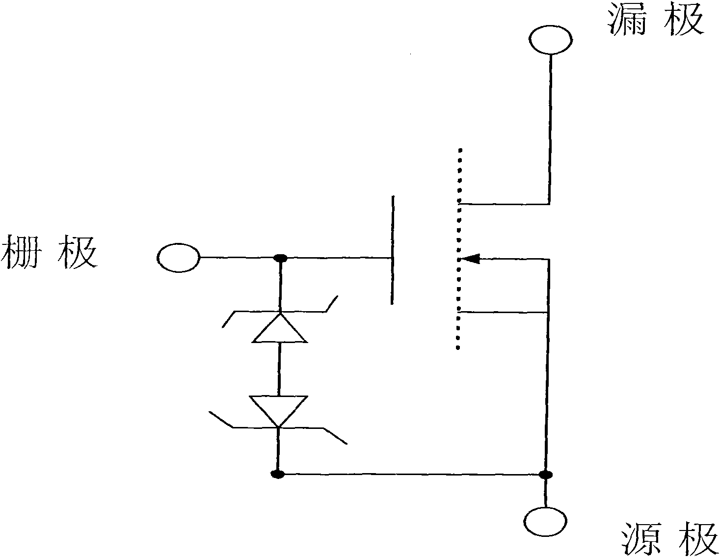
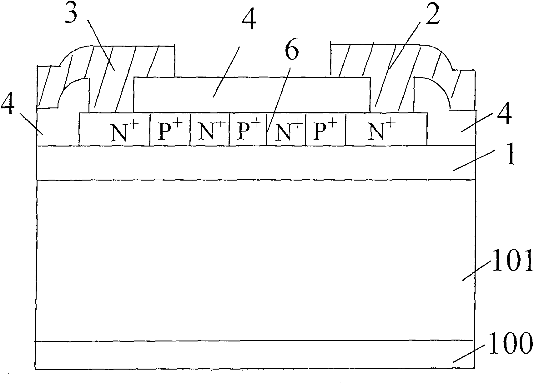
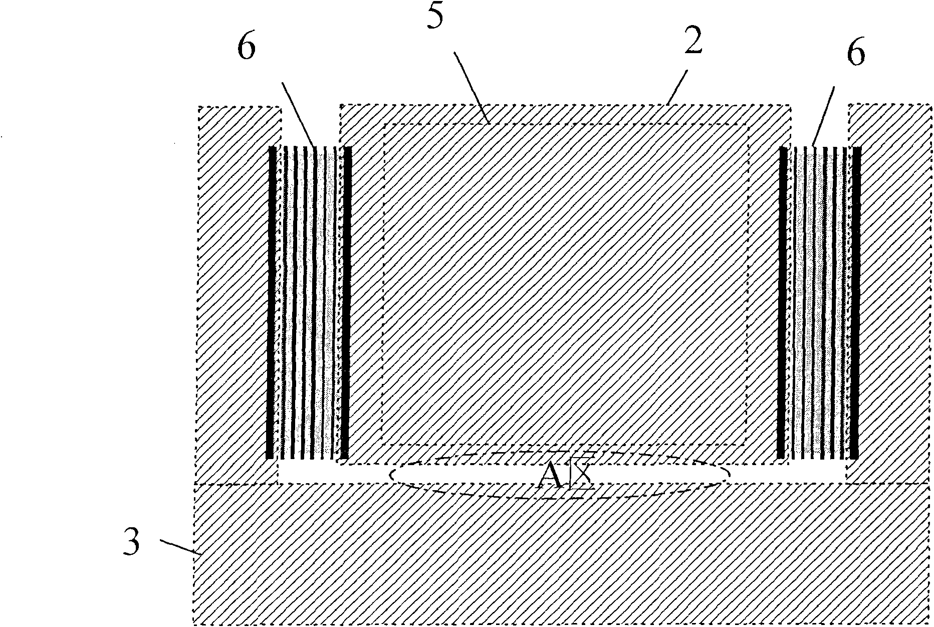
[0037] Embodiment 1: see attached Figure 5 , 9 , the ESD protection unit of the present invention integrated ESD protection power MOSFET, from bottom to top: substrate 100, epitaxial layer 101, oxide layer 1, polysilicon diode group 7, dielectric layer 4, gate metal 2 and source metal 3 . Gate metal 2 and N at one end of polysilicon diode group 7 + The doped region is connected to the gate of the power MOSFET, the source metal 3 is connected to the other end N of the polysilicon diode group 7 + Doped region and power MOSFET source connection. There may be a passivation layer (not shown in the figure) on the gate metal 2 and the original metal 3 . The ESD protection unit is disposed on the gate bonding area of ​​the power MOSFET and half surrounds the gate bonding area 5 between the cells.

[0038] Preparation: According to the usual power MOSFET preparation process, for example: use 920°C wet oxygen oxidation to grow about 500A pre-oxidation, and then perform photolithog...

Embodiment 2

[0039] Embodiment 2: as embodiment 1, wherein the power MOSFET source N + The advancing temperature was changed from 950°C to 970°C, and the time was changed from 150 minutes to 180 minutes, which reduced the gate-source breakdown voltage.

Embodiment 3

[0040] Embodiment 3: see Image 6 , as in Embodiment 1 or 2, wherein the P at one end of the polycrystalline diode group 7 + The doped region is connected to the gate of the power MOSFET, the source metal 3 is connected to the other end P of the polysilicon diode group 7 + Doped region and power MOSFET source connection. The two ends of the polycrystalline diode group of the ESD protection unit are P-type regions, and the P-type regions at both ends are composed of P - / P + structure composition, and P + At the outermost end of the diode group, the remaining P regions of the polycrystalline diode group are connected to the P - / P + P in the structure - the same, N + The dose to the zone is 5E15cm -2 -1.5E16cm -2 , P + The dose is 5E14cm -2 -8E15cm -2 . P + The advance time is 90 minutes.


PUM


Abstract

The invention improves the ESD protection integrated power MOSFET or IGBT. The invention is characterized in that the concentration of all P type areas in a poly-crystal diode set in an ESD protection unit is as same as the P type concentration of the power MOSFET or IGBT; the concentration of the N type area is as same as the N+ source of the power MOSFET or IGBT; the poly-crystal diode set is semi-circled around a grid bonding area between the grid bonding area and a structure cell area. If being a grid inserting structure, the middle of the semi-circled poly-crystal diode set is separated by the grid inserting structure so as to form left and right L-shaped parts which are disconnected, wherein all the P type areas and the N type areas in the poly-crystal diode are respectively formed by injecting and spreading the P well and N+ source of the power MOSFET or IGBT. The leakage between the grid and source electrodes of the acquired ESD protection integrated power MOSFET or IGBT is small. When preparing, a breakdown voltage between the grid and source electrodes is adjustable, the ESD discharging capability is high, the reliability is high and the manufacture is simple.

Description

technical field [0001] The invention improves the power MOSFET or IGBT with integrated ESD protection, and particularly relates to a kind of electric leakage between the gate and the source is small, the breakdown voltage between the gate and the source is adjustable during preparation, the ESD discharge capacity is high, and the reliability is good. Manufacture of simple integrated ESD protection power MOSFET or IGBT and preparation method. Background technique [0002] With the development of power semiconductor devices, people have higher requirements on the performance of power MOSFETs or IGBTs. For example, electrostatic (ESD) phenomena are often prone to occur during device packaging, transportation, assembly and use. A high electric field causes insulation breakdown of the gate dielectric under the high electric field, thereby causing the device to fail. Therefore, the electrostatic protection (ESD) protection function is one of the important indicators. Electrostati...

Claims


Application Information

Patent Timeline
Patent Type & Authority Applications(China)
IPC IPC(8): H01L27/02H01L29/861H01L29/06H01L21/77
Inventor 钱梦亮陈俊标李泽宏
Owner 江苏东晨电子科技有限公司
Why Eureka
Try Eureka