Doping method and method of manufacturing field effect transistor

a manufacturing method and transistor technology, applied in the direction of semiconductor devices, electrical appliances, basic electric elements, etc., can solve the problems of inability to detect the desired ion species by the above mass spectrometer, and difficulty in precisely controlling the doze amount of a desired ion species, so as to reduce the variation of the concentration of desired ions and reduce the variation of the threshold voltage

Inactive Publication Date: 2008-10-28
SEMICON ENERGY LAB CO LTD
View PDF42 Cites 7 Cited by
  • Summary
  • Abstract
  • Description
  • Claims
  • Application Information

AI Technical Summary

Benefits of technology

[0034]Comparing with a case of performing only the second plasma treatment without the first plasma treatment, the case of performing the first plasma treatment can reduce the variation of the concentration of a donor impurity or an acceptor impurity in the processing object which has been subjected to the doping process; accordingly, the variation of sheet resistance in the object can be reduced.
[0035]In accordance with the invention disclosed in this specification, the following effects can be obtained.
[0037]2) The variation of the threshold voltage of the manufactured field effect transistor can be reduced.
[0038]3) The variation of the peak concentration of a donor impurity or an acceptor impurity in a processing object, which has been subjected to a doping process, can be reduced by using an ion doping apparatus.
[0039]4) Even when doping is performed at a low concentration as in the case of channel doping, since an ion implantation apparatus is not needed, the manufacturing cost of a field effect transistor can be reduced.
[0040]5) When the concentration of the compound of the donor impurity or the acceptor impurity included in the source gas which is introduced to an ion doping apparatus is changed from the first concentration to the second concentration which is lower than the first concentration, the second concentration after the change can easily become stable.

Problems solved by technology

Accordingly, the doze amount is counted by not only a desired ion species but also total ions including an unnecessary ion species, which makes it difficult to precisely control the doze amount of a desired ion species.
However, the ion implantation apparatus is sometimes used only in a step of channel doping since the precise control is difficult to be performed with the ion doping apparatus.
However, when doping of boron at a low concentration is performed as in the case of channel doping, there is a problem in which ions of a compound including boron, in other words, a desired ion species is not detected by the above mass spectrometer.

Method used


Image

  • Doping method and method of manufacturing field effect transistor
  • Doping method and method of manufacturing field effect transistor
  • Doping method and method of manufacturing field effect transistor

Examples


embodiment modes

(Embodiment Mode 1)

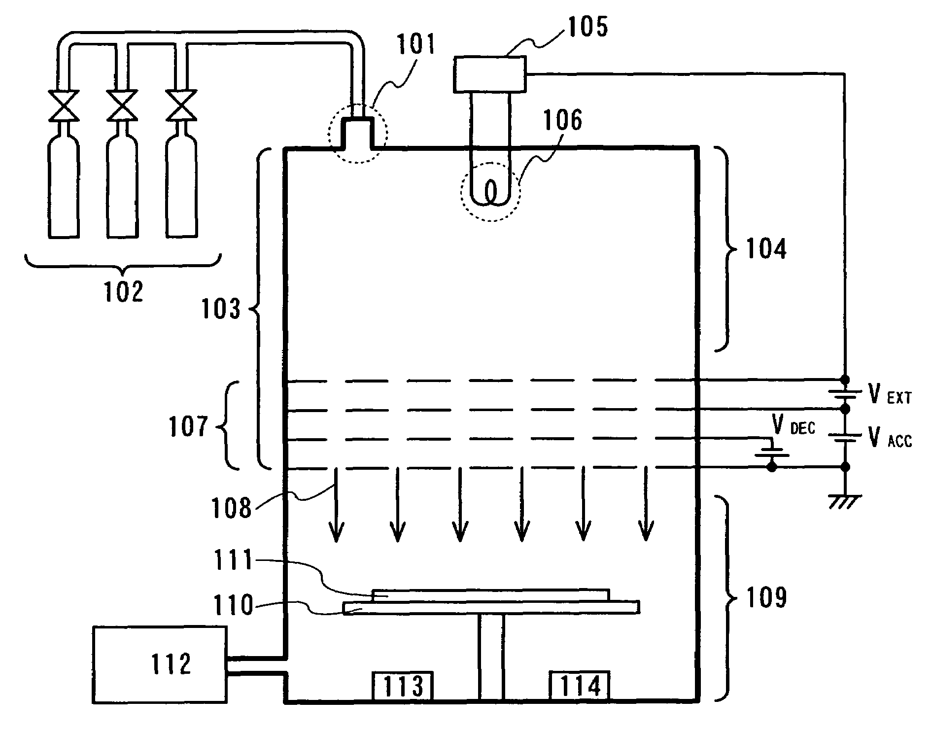
[0051]An example of an ion doping apparatus used in the invention disclosed in this specification will be described with reference to FIG. 1.

[0052]FIG. 1 is a schematic view of an ion doping apparatus. A gas introduction port 101 is connected to a gas supply system 102 which can supply a source gas, in which B2H6 is diluted with hydrogen or a rare gas (such as helium or argon), hydrogen, or a rare gas. The source gas, hydrogen, or the rare gas is introduced to a plasma generating portion 104 in an ion source 103 from the gas supply system 102 to generate plasma in the plasma generating portion 104. The ion source 103 further includes a discharge generating means 106 and an electrode portion 107. The electrode portion 107 includes an extraction electrode, an accelerating electrode, a decelerating electrode, and an earth electrode. The electrode portion 107 is also referred to as an extraction electrode system, and the above four electrodes are each provided with a ...

embodiment mode 2

(Embodiment Mode 2)

[0071]When an n-channel thin film transistor is manufactured using an ion doping apparatus in a step of channel doping, steps to obtain a dose amount of total ions in channel doping, required to approximate a threshold voltage Vth of the n-channel thin film transistor to a predetermined value (in this embodiment mode, +1.0 V), are carried out. The process is described below.

[0072]According to Formula 2 obtained in Embodiment Mode 1 of this specification, a peak concentration Y of boron in a semiconductor film (used as an active layer) containing silicon as its main component, required to obtain a threshold voltage of +1.0 V is 5.3×1017 cm−3.

[0073]In the case where a proportion X of B2Hy+ ions is 0.30, X of 0.30 and Y of 5.3×1017 cm−3 are assigned to Formula 1′ obtained in Embodiment Mode 1; accordingly, D1=1.0×1014 cm−2 can be obtained. From this result, it is found that a dose amount D1 of total ions in channel doping, required to obtain a threshold voltage Vth, ...

embodiment mode 3

(Embodiment Mode 3)

[0079]After performing channel doping to a semiconductor film containing silicon as its main component by using an ion doping apparatus, steps of obtaining the dose amount of total ions in doping are carried out, which is required to approximate a peak concentration of boron in the semiconductor film obtained by a result of analysis by SIMS to a desired value (in this embodiment mode, 4.4×1017 cm−3). The steps are described below

[0080]When a proportion X of B2Hy+ ions is 0.30, Y of 4.4×1017 cm−3 is assigned to Formula 1′ obtained in Embodiment Mode 1; accordingly, D1 of 8.4×1013 cm−2 can be obtained. From this result, a dose amount D1 of total ions required to obtain a peak concentration of boron of 4.4×1017 cm−3 in a semiconductor film containing silicon as its main component is found to be 8.4×1013 cm−2. Note that a source gas used in the channel doping step is B2H6 diluted with hydrogen to a concentration of 1%, which is used to obtain Formula 1 and Formula 1′ ...


PUM


Abstract

A doping method comprising the steps of; obtaining a proportion X of ions of a compound including a donor or an acceptor impurity in total ions from mass spectrum by using a first source gas of a first concentration; analyzing a peak concentration Y of the compound in a first processing object which is doped by using a second source gas of a second concentration equal to or lower than the first concentration, referring to a dose amount of total ions as D0 and setting an acceleration voltage at a value, obtaining a dose amount D1 of total ions from a expression, Y=(D1 / D0)(aX+b), and doping a second processing object with the donor or the acceptor impurity by a ion doping apparatus using a third source gas, wherein a dose amount of total ions is set at D1, and an acceleration voltage is set at the value.

Description

BACKGROUND OF THE INVENTION[0001]1. Field of the Invention[0002]The present invention disclosed in this specification relates to a doping method using an ion doping apparatus which does not require mass separation of generated ions and a method of manufacturing a field effect transistor using the doping method.[0003]2. Description of the Related Art[0004]In a manufacturing process of a semiconductor element such as a field effect transistor, when a donor impurity or an acceptor impurity is added into a processing object such as a semiconductor film formed over a substrate having an insulating surface or a semiconductor substrate, an ion implantation apparatus or an ion doping apparatus is used. An ion implantation apparatus is a mass-separation type apparatus in which an unnecessary ion species can be separated by using a mass separator and in which a processing object placed in a treatment chamber can be subjected to only a desired ion species. Therefore, the dose amount of a desir...

Claims


Application Information

Patent Timeline
Patent Type & Authority Patents(United States)
IPC IPC(8): H01L21/425
CPCH01L21/26513H01L29/66757H01L29/78621H01L21/2658
Inventor KOEZUKA, JUNICHISUZUKI, NAOKI
Owner SEMICON ENERGY LAB CO LTD
Why Eureka
Try Eureka