A trench-structured vdmos

A trench and inner trench technology, applied in semiconductor devices, electrical components, circuits, etc., can solve the problems of restricting reverse withstand voltage, affecting device dynamic characteristics, source-drain capacitance Cds, etc., and improving reverse blocking voltage. , The effect of low gate-drain capacitance Cds and uniform lateral electric field distribution

Inactive Publication Date: 2018-10-26
UNIV OF ELECTRONICS SCI & TECH OF CHINA
View PDF6 Cites 0 Cited by
  • Summary
  • Abstract
  • Description
  • Claims
  • Application Information

AI Technical Summary

Problems solved by technology

However, the body field plate type VDMOS also has some disadvantages. The longitudinal electric field distribution in the drift region is as follows: figure 1 As shown, it can be seen that since the potential on the entire field plate is the same, the value of the longitudinal electric field in the drift region decreases along the vertical direction, which restricts the further improvement of the reverse withstand voltage
At the same time, since the body field plate is connected to the source of VDMOS, its source-drain capacitance Cds will be high, which affects the dynamic characteristics of the device

Method used


Image

  • A trench-structured vdmos
  • A trench-structured vdmos
  • A trench-structured vdmos

Examples


Embodiment 1

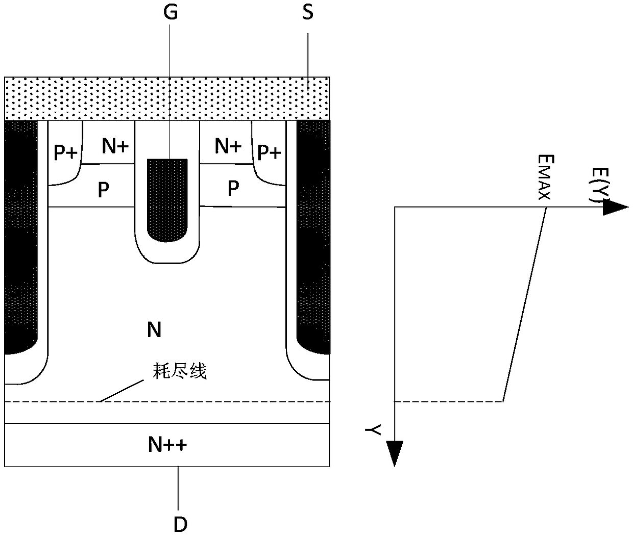
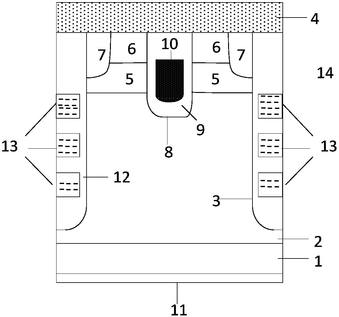
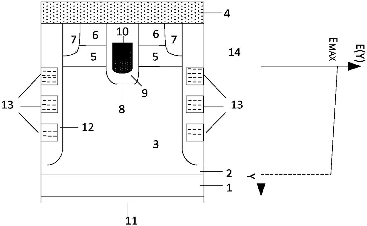
[0016] like image 3 As shown, a VDMOS with a trench structure in this example includes a metallized drain 11, an N+ substrate 1, an N-drift region 2, and a metallized source 4 that are sequentially stacked from bottom to top; Region 2 has internal trenches 3, P-type doped regions 5, N-type heavily doped regions 6, P-type heavily doped regions 7, and trenches 8, and the P-type doped regions 5 are located in the internal trenches on both sides. Between the grooves 3, and the side of the P-type doped region 5 is in contact with the side of the groove 3 in the body; the N-type heavily doped region 6 is located on the upper surface of the P-type doped region 5, and the N-type heavily doped region 6 The upper surface is in contact with the lower surface of the metallized source electrode 4; the P-type heavily doped region 7 is located between the internal trench 3 and the N-type heavily doped region 6 and is located between the internal trench 3 and the N-type heavily doped region ...

Embodiment 2

[0036] The structure of this example is based on Example 1. All N-type materials in Example 1 are replaced with P-type materials, all P-type materials are replaced with N-type materials, and negative charges in the polysilicon 13 are replaced with positive charges.

[0037] When making devices, semiconductor materials such as silicon carbide, gallium arsenide, or silicon germanium can also be used instead of silicon.


PUM


Abstract

The invention belongs to the technical field of semiconductors, in particular to a VDMOS device with a trench structure. The present invention mainly has two or more polysilicon islands wrapped by a silicon dioxide layer in the groove in the body, and negative charges are stored in these polysilicon islands. Since the polysilicon island is surrounded by an insulating layer, negative charges will be fixed within the polysilicon island. The density of negative charges stored in each polysilicon island varies, and the closer the polysilicon island is to the surface of the device, the higher the charge density is stored. When the device is reverse-blocked, a lateral electric field is generated between the high-potential N-type drift region and the negative charge in the polysilicon island, which assists in depleting the drift region. Since the potential of the N-type drift region gradually decreases from bottom to top, and the amount of negative charges increases from bottom to top, the lateral electric field distribution in the drift region is more uniform, so that the vertical electric field is closer to the rectangular distribution, improving the reverse blocking of the device Voltage. At the same time, since the body field plate structure connected to the source electrode is not used, the gate-to-drain capacitance Cds in the present invention is relatively low.

Description

technical field [0001] The invention belongs to the technical field of semiconductors, in particular to a VDMOS device with a trench structure. Background technique [0002] Power VDMOS is a multi-subconductor device, which has the advantages of fast switching speed, high input impedance, and easy driving. An ideal VDMOS should have low on-resistance, switching loss and high blocking voltage. However, there is a restraint effect between on-resistance and breakdown voltage, on-resistance and switching loss, which limits the development of power VDMOS. In order to improve device performance and reduce on-resistance, academician Chen Xingbi proposed a super-junction VDMOS structure. Compared with the traditional structure, the super-junction structure obtains a better trade-off relationship between device withstand voltage and on-resistance. Under the same device withstand voltage condition, the on-resistance of VDMOS with super-junction structure is smaller. [0003] Since ...

Claims


Application Information

Patent Timeline
Patent Type & Authority Patents(China)
IPC IPC(8): H01L29/78H01L29/06
CPCH01L29/0657H01L29/7802
Inventor 任敏李爽李家驹罗蕾李泽宏张金平高巍张波
Owner UNIV OF ELECTRONICS SCI & TECH OF CHINA
Why Eureka
Try Eureka