Array substrate and preparation method thereof, flexible display device

An array substrate and substrate technology, which is applied in nonlinear optics, semiconductor/solid-state device manufacturing, instruments, etc., and can solve problems such as line breakage and short circuit

Active Publication Date: 2018-01-09
BOE TECH GRP CO LTD
View PDF4 Cites 30 Cited by
  • Summary
  • Abstract
  • Description
  • Claims
  • Application Information

AI Technical Summary

Problems solved by technology

[0009] Embodiments of the present invention provide an array substrate and its preparation method, and a flexible display device, which are us

Method used


Image

  • Array substrate and preparation method thereof, flexible display device
  • Array substrate and preparation method thereof, flexible display device
  • Array substrate and preparation method thereof, flexible display device

Examples


Embodiment Construction

[0045] The following will clearly and completely describe the technical solutions in the embodiments of the present invention with reference to the accompanying drawings in the embodiments of the present invention. Obviously, the described embodiments are only some, not all, embodiments of the present invention. Based on the embodiments of the present invention, all other embodiments obtained by persons of ordinary skill in the art without making creative efforts belong to the protection scope of the present invention.

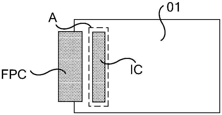
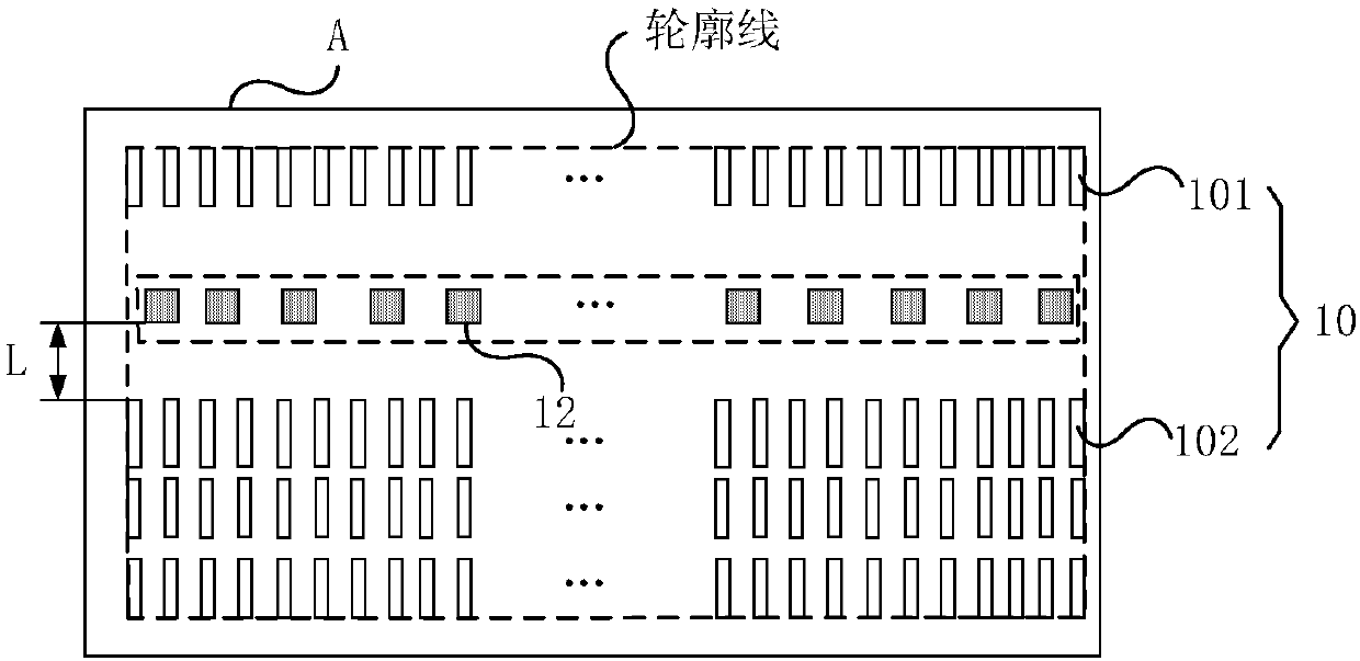
[0046] An embodiment of the present invention provides an array substrate, image 3 The structure of the binding region A of the array substrate is shown. The array substrate includes a binding area A, and a plurality of binding pads 10 arranged in the binding area of ​​the flexible substrate 11, wherein the binding pads 10 are such as Figure 4 As shown, bond pin 42 for bonding IC. The array substrate further includes: an insulating support portion 12 locat...


PUM


Abstract

An embodiment of the invention provides an array substrate and a preparation method thereof, and a flexible display device, relates to the technical field of flexible display and is used for solving aproblem of proneness of circuit breakage and short circuit when an IC is bound to the flexible display panel directly. The array substrate including a binding area and a plurality of binding bondingpad arranged in the binding area of the flexible substrate. The array substrate also includes an insulation support part disposed in the binding area and in a position without the binding bonding pad.The upper surface of the insulation support part protrudes from the upper surface of the binding bonding pad. The array substrate is used for forming the flexible display device.

Description

technical field [0001] The present invention relates to the technical field of flexible display, in particular to an array substrate, a preparation method thereof, and a flexible display device. Background technique [0002] With the development of display technology, more and more electronic devices begin to use flexible display panels that are thin and have good impact resistance properties. Display devices that use flexible display panels include liquid crystal display devices, organic electroluminescent display devices, and electrophoretic displays. device. The flexible display device can be applied to smart cards, portable computers, electronic paper, and the like. At present, the preparation process of flexible display panels has made great progress. [0003] When a flexible display device is manufactured, generally, a flexible substrate is disposed on a glass substrate first, and then a layer structure required for display is fabricated on the flexible substrate to ...

Claims


Application Information

Patent Timeline
IPC IPC(8): H01L27/12H01L27/32H01L51/56
CPCH01L27/12G02F1/1333H01L2224/81203H01L2224/83851H01L2224/16238H01L2224/81191H01L2224/8114H01L2224/10165H01L24/81H01L24/16H01L2224/81903H01L2224/9211H10K59/129H01L2924/00014H01L2224/81H01L2224/83H01L21/4853H01L21/4857H01L23/49811H01L23/49838H01L23/4985H01L2224/16227H01L2224/81005
Inventor 陈立强王红丽王艳丽王有为李建伟蔡宝鸣
Owner BOE TECH GRP CO LTD
Why Eureka
Try Eureka