Fingerprint detection circuit, detection method of fingerprint detection circuit and fingerprint sensor

A fingerprint detection and circuit technology, which is applied in the direction of acquiring/organizing fingerprints/palmprints, circuits, instruments, etc., can solve the problems of threshold voltage value drift, detection circuit cannot detect fingerprints normally, detection circuit output data drift, etc., to avoid drift , ideal follow-up effect, and the effect of improving the signal-to-noise ratio

Active Publication Date: 2018-01-12
BOE TECH GRP CO LTD
View PDF16 Cites 11 Cited by
  • Summary
  • Abstract
  • Description
  • Claims
  • Application Information

AI Technical Summary

Problems solved by technology

[0004] However, for the glass-on-glass amorphous silicon process or low-temperature polysilicon process, the voltage follower transistor in the active fingerprint detection circuit will use a thin film transistor. Due to the influence of the characteristics of the thin film transistor itself, its threshold voltage will change with time. Drift occurs, which makes the following effect of the voltage follower transistor unsatisfactory, resulting in drift of the output data of the detection circuit, which causes the detection circuit to fail to detect fingerprints normally

Method used


Image

  • Fingerprint detection circuit, detection method of fingerprint detection circuit and fingerprint sensor
  • Fingerprint detection circuit, detection method of fingerprint detection circuit and fingerprint sensor
  • Fingerprint detection circuit, detection method of fingerprint detection circuit and fingerprint sensor

Examples


Embodiment Construction

[0061] In order to further explain the technical means and effects of the present invention to achieve the intended purpose of the invention, the specific implementation of the fingerprint detection circuit, the detection method of the fingerprint detection circuit and the fingerprint sensor of the application of the present invention will be described below in conjunction with the accompanying drawings and preferred embodiments. , structure, characteristics and functions are described in detail. In the following description, different "one embodiment" or "embodiment" do not necessarily refer to the same embodiment. Furthermore, the particular features, structures, or characteristics of one or more embodiments may be combined in any suitable manner.

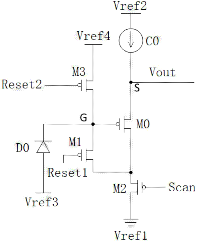
[0062] Such as figure 1 As shown, the embodiment of the present invention provides a fingerprint detection circuit, the fingerprint detection circuit has a scanning signal terminal Scan and a signal output terminal Vout, which i...


PUM


Abstract

The invention discloses a fingerprint detection circuit, a detection method of the fingerprint detection circuit and a fingerprint sensor, and relates to the technical field of fingerprint identification. The main purpose of the fingerprint detection circuit is to enable the detection circuit to normally detect a fingerprint. According to the main technical scheme, the fingerprint detection circuit comprises a photosensitive unit, a voltage following transistor, a first switch transistor and a second switch transistor. The gate of the first switch transistor is connected with a first reset control terminal. The first electrode of the first switch transistor is connected with a node while the second electrode of the first switch transistor is connected with the second electrode of the voltage following transistor. The gate of the second switch transistor is connected with a scanning signal terminal. The first electrode of the second switch transistor is connected with the second electrode of the transistor while the second electrode of the second switch transistor is connected with a reference voltage terminal. The gate of the voltage following transistor is connected with the node.The first electrode of the voltage following transistor is connected with a signal output terminal and is further connected with a second reference voltage terminal through a current source. The first electrode of the photosensitive unit is connected with a third reference voltage terminal while the second electrode is connected with the node. The fingerprint detection circuit, the detection method of fingerprint detection circuit and the fingerprint sensor are mainly used for fingerprint detection.

Description

technical field [0001] The invention relates to the technical field of fingerprint identification, in particular to a fingerprint detection circuit, a detection method of the fingerprint detection circuit and a fingerprint sensor. Background technique [0002] Optical fingerprint recognition devices have the advantages of long-distance sensing and have been widely used. Moreover, in order to reduce the noise of fingerprint detection results, optical fingerprint sensors usually use active detection circuits for detecting voltages to detect fingerprints. [0003] The existing active fingerprint detection circuit usually includes a first switching transistor and a photodiode connected in series with it, and a voltage following transistor and a second switching transistor connected in series. The voltage is reset, and the gate voltage changed due to the illumination of the photodiode is followed and output to the column output bus through the source of the voltage follower trans...

Claims


Application Information

Patent Timeline
Patent Type & Authority Applications(China)
IPC IPC(8): G06K9/00
CPCG06F3/042G06V40/1318G06F3/0304H01L31/0224H01L29/42356
Inventor 王鹏鹏王海生丁小梁郑智仁韩艳玲刘伟曹学友
Owner BOE TECH GRP CO LTD
Why Eureka
Try Eureka