
Structure for improving stacking mounting of multiple chips and technological method of structure

A process method and multi-chip technology, applied in the direction of electrical components, electrical solid devices, circuits, etc., can solve the problems of chip cover, chip breakage, etc., to achieve the effect of convenient layout, improved utilization, and improved process methods

Pending Publication Date: 2018-01-12
JCET GROUP CO LTD
View PDF0 Cites 0 Cited by
  • Summary
  • Abstract
  • Description
  • Claims
  • Application Information

AI Technical Summary

Problems solved by technology

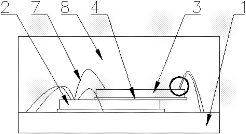
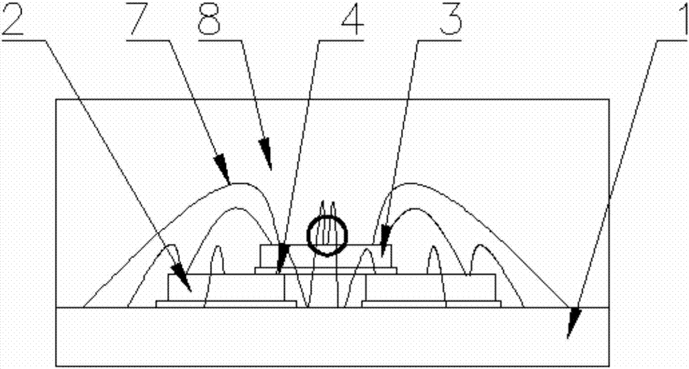
[0005] The technical problem to be solved by the present invention is to provide an improved multi-chip stacking chip loading structure and its process method in view of the above-mentioned prior art. In a limited space, it can effectively enhance the ability of multi-chip chip loading, increase the space Utilization rate, avoiding the problem of chip breakage due to insufficient strength in the suspended wire bonding area, and also avoiding the problem that part of the wire bonding area of ​​the lower chip is easily covered by the upper chip due to insufficient space

Method used


Image

  • Structure for improving stacking mounting of multiple chips and technological method of structure
  • Structure for improving stacking mounting of multiple chips and technological method of structure
  • Structure for improving stacking mounting of multiple chips and technological method of structure

Examples


Embodiment 1

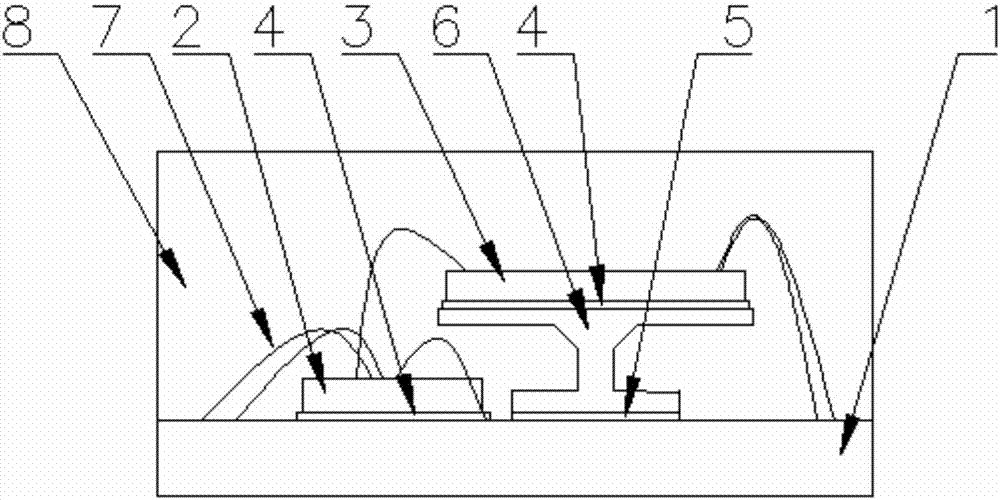
[0047] Such as image 3 As shown, an improved multi-chip stacking structure in this embodiment includes a frame base material 1, and the front side of the frame base material 1 is provided with a lower chip 2 through a die-mounting glue 4, and the frame base material 1 The front side is provided with an "I"-shaped bracket 6 through the film 5, and the front side of the "I"-shaped bracket 6 is provided with an upper chip 3 through a mounting glue 4. The frame substrate 1, the lower chip 2 and the upper chip 3 All are connected by bonding wires 7, and the lower chip 2, the upper chip 3, the "I"-shaped bracket 6 and the bonding wires 7 are encapsulated with a plastic encapsulant 8;

[0048] The "I"-shaped support 6 is an "I"-shaped support with a large top and a small bottom, and the area and height of the top surface and the bottom surface are customized according to the actual chip specifications, package thickness, and wiring capability;

[0049] Part of the area of ​​the low...

Embodiment 2

[0063] see Figure 11 The difference between Embodiment 2 and Embodiment 1 is that there are multiple lower-layer chips 2 .

[0064] Its process method comprises the following steps:

[0065] Step 1, see Figure 12 , take a frame substrate;

[0066] Step two, see Figure 13 , mounting multiple lower-layer chips on the frame substrate;

[0067] Step three, see Figure 14 , mount the "I"-shaped bracket on the frame substrate;

[0068] Step 4, see Figure 15 , Mount the upper chip on the "I"-shaped bracket;

[0069] Step five, see Figure 16 , the frame base material, the lower chip and the upper chip are all connected by bonding wires;

[0070] Step six, see Figure 17 , encapsulation.

[0071] Or its processing method comprises the steps:

[0072] Step 1, see Figure 18 , take a frame substrate;

[0073] Step two, see Figure 19 , mounting multiple lower-layer chips on the frame substrate;

[0074] Step three, see Figure 20 , wire bonding operation between the l...


PUM


Abstract

The invention discloses a structure for improving stacking mounting of multiple chips and a technological method of the structure. The structure comprises a frame base material (1); the front side ofthe frame base material (1) is provided with a lower layer chip (2) and an H-shaped support (6); an upper layer chip (3) is arranged on the front side of the H-shaped support (6); the frame base material (1), the lower layer chip (2) and the upper layer chip (3) are connected through welding lines (7); the lower layer chip (2), an upper layer chip (3), the H-shaped support (6) and the welding lines (7) are coated with a plastic packaging material (8). The invention provides the structure for improving stacking mounting of the chips and the technological method of the structure. The space utilization rate can be increased as much as possible in the same size of packaging, more convenient layout can be achieved, the problem that partial areas of the upper layer chip are arranged in a suspended mode is avoided, and the problem that part of a routing area of the lower layer chip is covered with the upper layer chip is avoided.

Description

technical field [0001] The invention relates to a structure for improving multi-chip stacking chip loading and a process method thereof, belonging to the technical field of semiconductor packaging. Background technique [0002] At present, the development trend of semiconductor products is miniaturization and densification, installing as many chips as possible in the smallest possible area, reducing space occupation, and improving space utilization, and the packaging required by customers generally has size requirements, so the product's The package size is limited. For the same package size, multi-chip stacking can effectively reduce the package size and meet the current development trend. There are some problems with multi-chip packaging. At present, there are the following types: [0003] 1. When loading multiple chips, the loading area is not large enough to meet the conditions. At this time, the chip or frame needs to be redesigned, and the required requirements may not...

Claims


Application Information

Patent Timeline
IPC IPC(8): H01L23/13H01L23/00H01L25/00H01L21/60
CPCH01L2224/48091H01L2224/48137H01L2224/49109H01L2224/73265H01L2924/00014
Inventor 缪江黔刘敏朱仲明
Owner JCET GROUP CO LTD
Learn More