Defect correction method of active matrix substrate and manufacturing method of display device

A technology of active matrix and manufacturing method, applied in optics, instruments, electrical components, etc., can solve problems such as defective liquid crystal display equipment and reduce the qualified rate of liquid crystal display equipment manufacturing

Inactive Publication Date: 2018-01-16
HKC CORP LTD
View PDF6 Cites 5 Cited by
  • Summary
  • Abstract
  • Description
  • Claims
  • Application Information

AI Technical Summary

Problems solved by technology

If the number of missing linear dots increases, the liquid crystal display device will become defective, and the manufacturing pass rate of the liquid crystal display device will be reduced.

Method used


Image

  • Defect correction method of active matrix substrate and manufacturing method of display device
  • Defect correction method of active matrix substrate and manufacturing method of display device
  • Defect correction method of active matrix substrate and manufacturing method of display device

Examples


Embodiment Construction

[0039] The technical solutions in the embodiments of the present application will be clearly and completely described below in conjunction with the drawings in the embodiments of the present application. Apparently, the described embodiments are some of the embodiments of the present application, but not all of them. Based on the embodiments in this application, all other embodiments obtained by persons of ordinary skill in the art without making creative efforts belong to the scope of protection of this application.

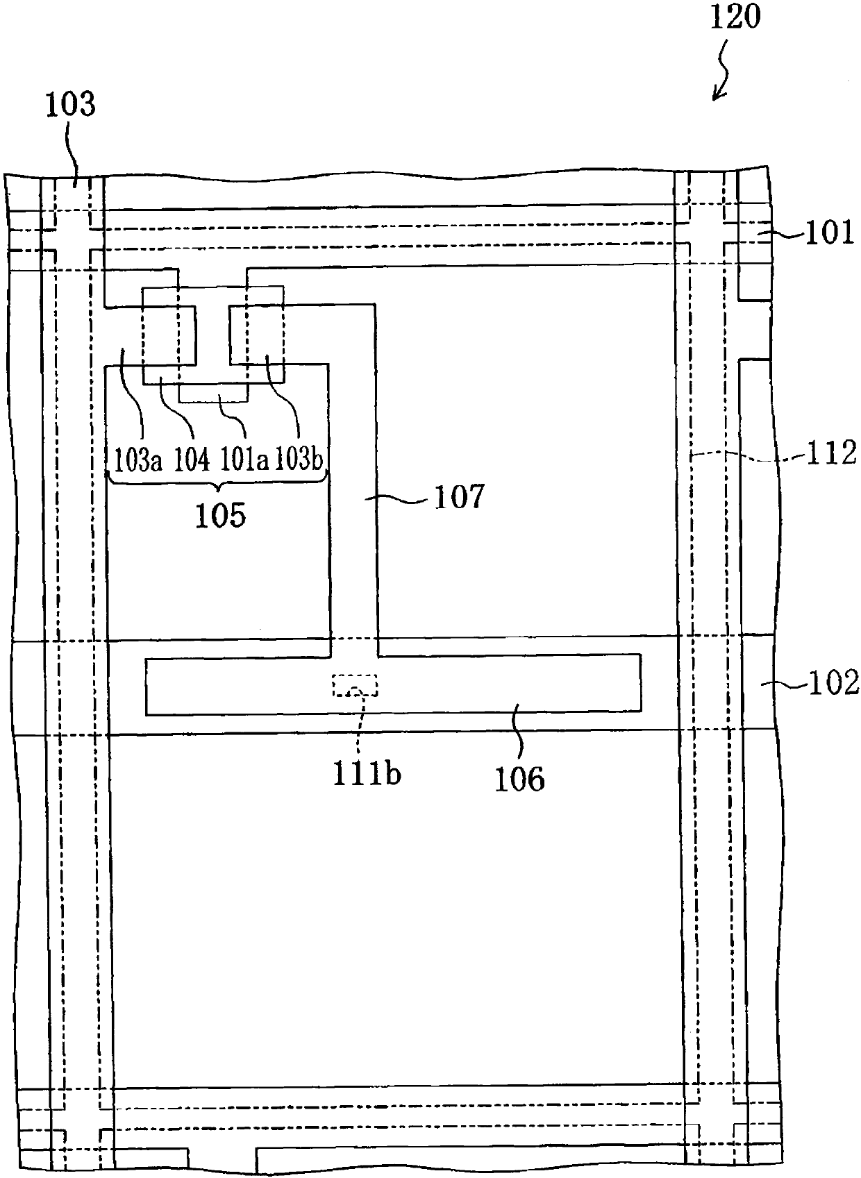
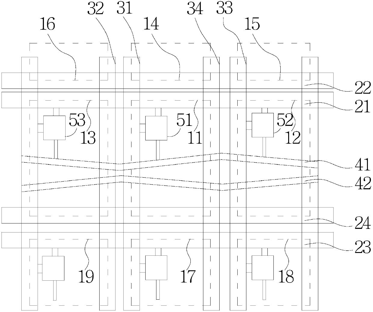
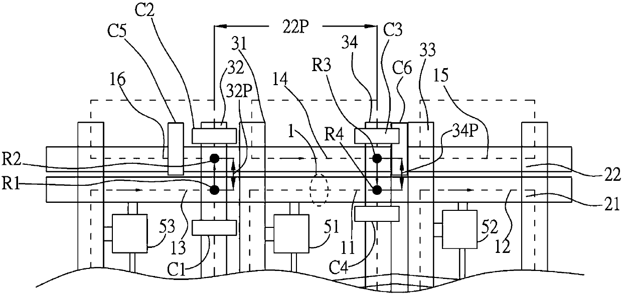
[0040] figure 1 For a plan view of the bottom of an active matrix village in an embodiment of the present application, please refer to figure 1 , an active matrix substrate, comprising: a substrate; a plurality of pixel electrodes 11, 12, 13, 14, 15, 16, 17, 18, 19 arranged on the substrate and forming a matrix to form each pixel, a plurality of The first gate lines 21, 23 are respectively arranged between the pixel electrodes 11, 12, 13, 14, 15, 16, 17, 18,...


PUM


Abstract

The invention provides a defect correction method of an active matrix substrate. The method comprises the broken line detection process, whether or not a broken line exists in first gate lines and second gate lines is detected, if it is detected that the first gate lines have a broken line, the portions, beyond the broken first gate line and the portions beyond the second gate lines adjacent to the broken first gate line are cut along all second source lines which are arranged on two sides of a pixel electrode corresponding to the broken line portion of the first gate lines, source gate line repairing part forming processes of source gate line repairing parts which have the overlapped part of the first gate lines with the broken line and the second gate lines are formed respectively, amongthe second gate lines adjacent to the first gate lines with the broken line, the portions beyond all the second gate lines which are arranged along two sides of the pixel electrode corresponding to the broken portion are cut, and a gate line repairing part forming process of the gate line repairing parts which have the overlapped parts of all the second gate lines and a connecting process for connection are formed.

Description

technical field [0001] The present application relates to the technical field of liquid crystal display, in particular to a method for correcting defects of an active matrix substrate and a method for manufacturing a display device. Background technique [0002] The operation mode of the flat panel display is to control each pixel (pixel) arranged in an array by two sets of addressing lines perpendicular to each other, so as to achieve the purpose of display. In various display control modes, the gate line and the source line are most commonly used to turn on or off the corresponding switch components, so that the signal transmitted by each gate line can be written into the pixel, thereby changing The state of the corresponding pixel, and achieve the purpose of controlling the display screen. [0003] Figure 8 is a plan view showing one pixel of a conventional active matrix substrate 120 . The active matrix substrate 120 includes: a plurality of pixel electrodes 112 arran...

Claims


Application Information

Patent Timeline
Patent Type & Authority Applications(China)
IPC IPC(8): G02F1/1362
CPCH01L22/22H01L22/12H01L22/14H01L27/124G02F1/136263G02F1/136259G02F1/1368H01L27/1259
Inventor 何怀亮
Owner HKC CORP LTD
Why Eureka
Try Eureka