A circuit structure and method for expanding memory operation times

A technology of circuit structure and number of operations, applied in static memory, digital memory information, information storage, etc., can solve the problem that phase change memory cannot realize the read-write and erase balance of memory cells, and achieve the effect of avoiding excessive operation.

Active Publication Date: 2020-09-15
SHANGHAI INST OF MICROSYSTEM & INFORMATION TECH CHINESE ACAD OF SCI
View PDF5 Cites 0 Cited by
  • Summary
  • Abstract
  • Description
  • Claims
  • Application Information

AI Technical Summary

Problems solved by technology

[0006] In view of the shortcomings of the prior art described above, the purpose of the present invention is to provide a circuit structure and method for extending the number of operations of the memory, which is used to solve the problem that the phase change memory in the prior art cannot achieve read-write-erasing balance of each storage unit. question

Method used


Image

  • A circuit structure and method for expanding memory operation times
  • A circuit structure and method for expanding memory operation times
  • A circuit structure and method for expanding memory operation times

Examples


Embodiment 1

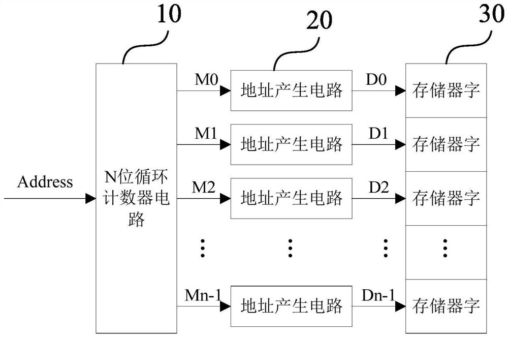
[0078] like figure 1 As shown, this embodiment provides a circuit structure for extending the number of memory operations, the circuit structure includes:

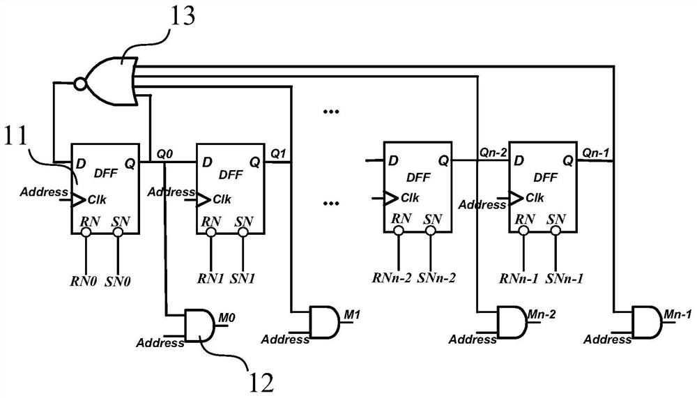
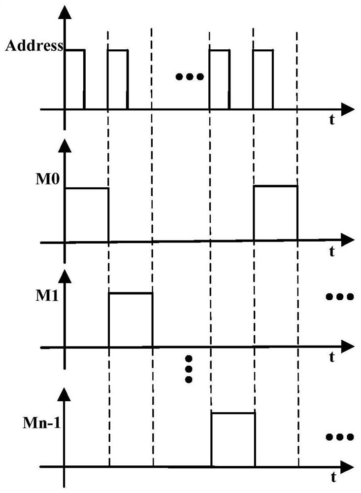
[0079] The N-bit cycle counter circuit 10 is used to sequentially generate an effective output signal at the N output terminals according to the input address pulse signal, and when the circuit structure is powered on, generate a set signal and a reset signal fed back by the circuit according to the address , restore the state of the N-bit cycle counter circuit to the state before power down;

[0080] N address generating circuits 20 are connected to the N-bit cycle counter circuit 10, and are used to make the N-bit cycle counter circuit work with the N-bit cycle counter circuit according to a valid output signal generated by an output terminal of the N-bit cycle counter circuit when the circuit structure works normally. The address generating circuit corresponding to the output terminal generates an address signal and ou...

Embodiment 2

[0105] This embodiment provides a method for extending the number of memory operations by using the circuit of the first embodiment, and the method includes:

[0106] When the circuit structure works normally, the N-bit cycle counter circuit sequentially generates a valid output signal at the N output terminals according to the input address pulse signal, and the N address generation circuits according to the N-bit cycle counter circuit An effective output signal generated by an output terminal causes the address generation circuit corresponding to the output terminal to generate and output an address signal, and the memory array will input the address signal to the memory array according to the address signal output by the address generation circuit The data is written into the memory word corresponding to the address signal, so that the input data is sequentially written into N memory words in a circular manner;

[0107] When the circuit structure is powered off, the N addre...


PUM


Abstract

The invention provides a circuit structure and method for expanding the number of operation times of a memory. The circuit structure comprises an N-bit cycle counter circuit, N address generation circuits and a memory array; the N address generation circuits are connected with the N-bit cycle counter circuit; the memory array is connected with the N address generation circuits; N times of operations on a memory word are dispersed into N different memory words; therefore, excessive operation on a memory word is avoided; when the power is off every time, the state of a trigger circuit is storedin a non-volatile phase change memory; when the power is on every time, the data in the non-volatile phase change memory is read out; therefore, the trigger circuit and the N-bit cycle counter circuitrecover to the state before the power is off; and thus, balanced operation of the memory words in any condition can be realized. By means of the circuit structure and method for expanding the numberof operation times of the memory provided by the invention, the problem that a phase change memory cannot realize the reading, writing and erasing balance of each memory unit in the prior art can be solved.

Description

technical field [0001] The invention belongs to the application field of integrated circuit memory, and in particular relates to a circuit structure and method for extending memory operation times. Background technique [0002] With the rapid development of informatization, networking and intelligence, the embedded storage system has become an important node of data processing. The number of times of writing and erasing is limited. When the number of times of reading, writing and erasing reaches a certain limit, the data stored in the memory will become unreliable. Moreover, with the improvement of integrated circuit technology, charge-type memories such as DRAM and Flash Memory generally have defects such as low write durability and low performance of memory cells, which have encountered development bottlenecks and limited their wide application. [0003] In order to increase the lifespan of the memory and make each bit of the memory cell obtain read-write and erase-balanc...

Claims


Application Information

Patent Timeline
Patent Type & Authority Patents(China)
IPC IPC(8): G11C13/00
Inventor 陈后鹏李喜王倩李晓云雷宇郭家树陈小刚宋志棠苗杰
Owner SHANGHAI INST OF MICROSYSTEM & INFORMATION TECH CHINESE ACAD OF SCI
Why Eureka
Try Eureka