ESD protection devices with SCR structures for semiconductor integrated circuits

Active Publication Date: 2006-04-20
RENESAS ELECTRONICS CORP
View PDF5 Cites 12 Cited by
  • Summary
  • Abstract
  • Description
  • Claims
  • Application Information

AI Technical Summary

Benefits of technology

[0016] According to the present invention, the uneven distribution of ESD current does not occur in the SCR part, achieving the uniform operation of SCR. There

Problems solved by technology

Therefore, in the example in FIG. 6, even if the unit element size (Wunit in FIG. 6) of the SCR is increased in order to enhance discharge ability, the effect of increasing the unit element size cannot be obtained because of the uneven distribution of the discharge current.
On the other hand, when Wunit is shorter than 10 μm, the ESD current does not flow sufficiently and desirable ESD protection characte

Method used


Image

  • ESD protection devices with SCR structures for semiconductor integrated circuits
  • ESD protection devices with SCR structures for semiconductor integrated circuits
  • ESD protection devices with SCR structures for semiconductor integrated circuits

Examples


example

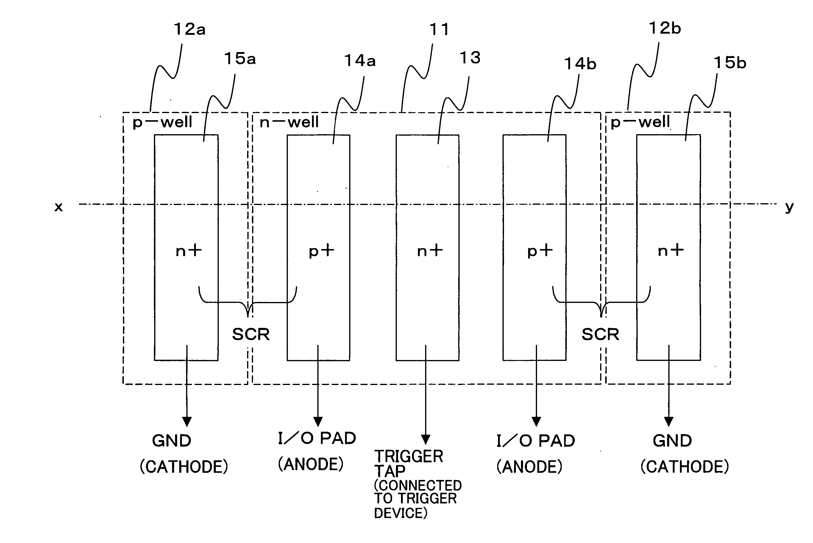
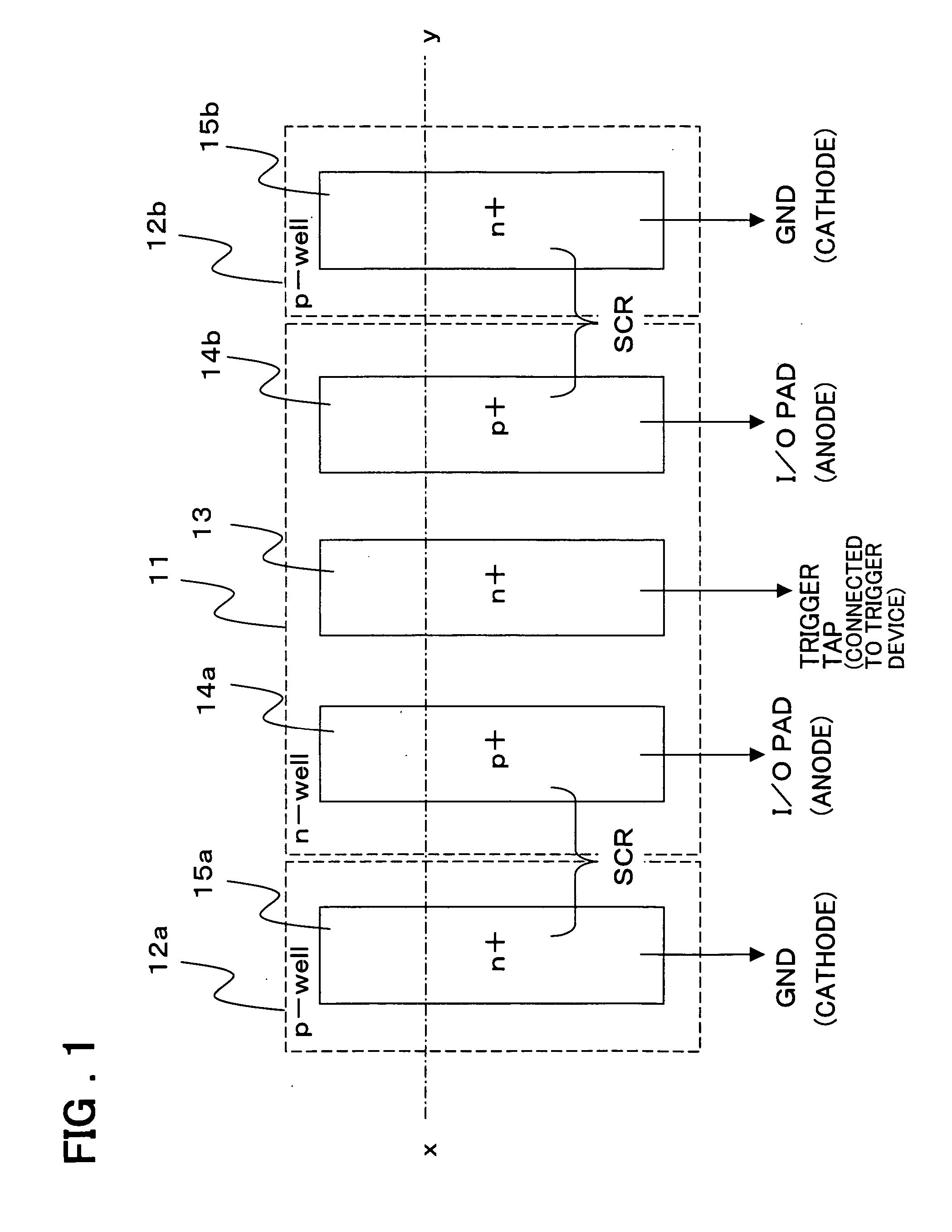
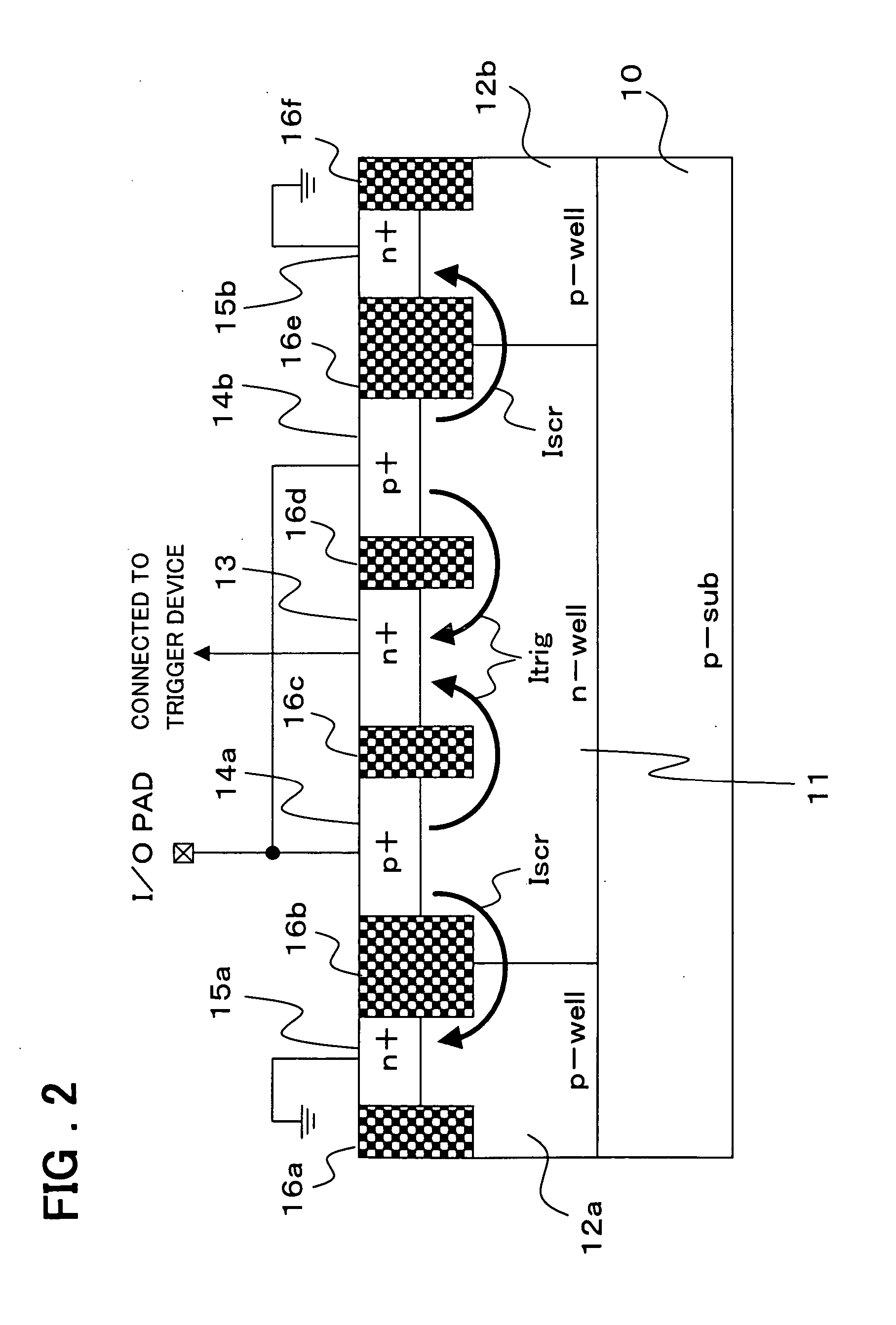
[0029]FIGS. 3A, 3B and 3C are layout diagrams showing each layer of the ESD protection circuit relating to an example of the present invention. FIG. 3A is a layout diagram corresponding to FIG. 1, and the rectangular N-type well 11 is formed in the center with the P-type wells 12 surrounding it. In the center of the N-type well 11, the rectangular high concentration N-type (N+) region 13, to which the trigger electrode is connected, is formed, and the rectangular high concentration P-type (P+) regions 14a and 14b, to which the anode electrode is connected, are formed symmetrically above and beneath this high concentration N-type region 13. Further, facing the high concentration P-type regions 14a and 14b, to which the anode electrode is connected, the rectangular high concentration N-type (N+) regions 15a and 15b, to which the cathode electrodes are connected respectively, are formed on the P-well 12. The high concentration N-type region 13, and the high concentration P-type regions...


PUM


Abstract

To control the uneven distribution of current density and reduce the area of an ESD protection circuit in an SCR-type ESD protection device. An N-type well 11, and P-type wells 12a and 12b disposed oppositely and adjacent to the N-type well 11, with the N-type well 11 interposed between them, are formed on the surface of a semiconductor substrate. A high concentration N-type region 15a is formed on the surface of the P-type well 12a, a high concentration N-type region 15b is formed on the surface of the P-type well 12b, and each of them is grounded. Further, a high concentration P-type region 14a is formed, oppositely to the high concentration N-type region 15a, on the surface of the N-type well 11, and a high concentration P-type region 14b is formed, oppositely to the high concentration N-type region 15b, on the surface of the N-type well 11, and each of them is connected to an I/O pad. A high concentration N-type region 13 is formed on the N-type well 11, being interposed between the high concentration P-type region 14a and the high concentration P-type region 14b, and connected to a trigger device. A surge loaded on the I/O pad is released to the ground terminal via the SCR structures on the both sides.

Description

FIELD OF THE INVENTION [0001] The present invention relates to a semiconductor integrated device and particularly a semiconductor integrated device comprising an ESD protection circuit. BACKGROUND OF THE INVENTION [0002] A semiconductor integrated circuit (IC) is required to be resistant to surge voltage and surge current caused by electrostatic discharge (ESD) and loaded on the input / output pad of the IC. In order to meet this requirement, an ESD protection circuit is connected to the input / output pad of IC in general. Such an ESD protection circuit is required to have a good discharge ability and low trigger voltage as semiconductor integrated circuits are miniaturized. An example of an ESD protection circuit that meets these requirements is disclosed in Patent-Document 1. [0003]FIG. 4 is a cross-sectional view showing the structure of the main part of a conventional ESD protection circuit. On a P-type semiconductor substrate 100, an N-type well 101 and a P-type well 102, adjacent...

Claims


Application Information

Patent Timeline
IPC IPC(8): H01L23/62
CPCH01L27/0262H01L29/7436
Inventor MORISHITA, YASUYUKI
Owner RENESAS ELECTRONICS CORP
Why Eureka
Try Eureka