Microfluidic chip device with polydimethylsiloxane as substrate material

A polydimethylsiloxane and microfluidic chip technology, applied in the field of analysis and testing, can solve the problems of large flow resistance, which have not been properly solved, and difficulties in the passage of fine liquid flow, so as to achieve the effect of eliminating troublesome procedures

Inactive Publication Date: 2018-02-02
洪小女
View PDF2 Cites 1 Cited by
  • Summary
  • Abstract
  • Description
  • Claims
  • Application Information

AI Technical Summary

Problems solved by technology

[0006] But it's not that simple
[0007] First, this polydimethylsiloxane material, the material referred to by the acronym PDMS, is itself a strongly hydrophobic material. Microchannels are built on this material. If the microchannels are not targeted The modification operation of the surface of the channel, then, after the overall assembly is completed, that is, after the cover is covered, because the inner surface of the micro channel in the structure occupies most of the inner surface of the liquid flow channel, then the PDMS micro channel The strong hydrophobic characteristic of the inner surface of the channel is the decisive factor, which will make it very difficult for the polar liquid flow similar to the aqueous solution to pass through, and its flow resistance is so large that even ordinary micropumps are difficult to push. Of course, If the cover sheet also chooses to use the PDMS material, then the problem is basically the same, with little difference; therefore, in the prior art, it is necessary to modify and modify the inner surface of the microchannel on the PDMS material; then , is this modification operation for the inner surface of the PDMS microchannel very troublesome? That's not the problem. What constitutes a serious technical problem i

Method used


Image

  • Microfluidic chip device with polydimethylsiloxane as substrate material

Examples


Embodiment Construction

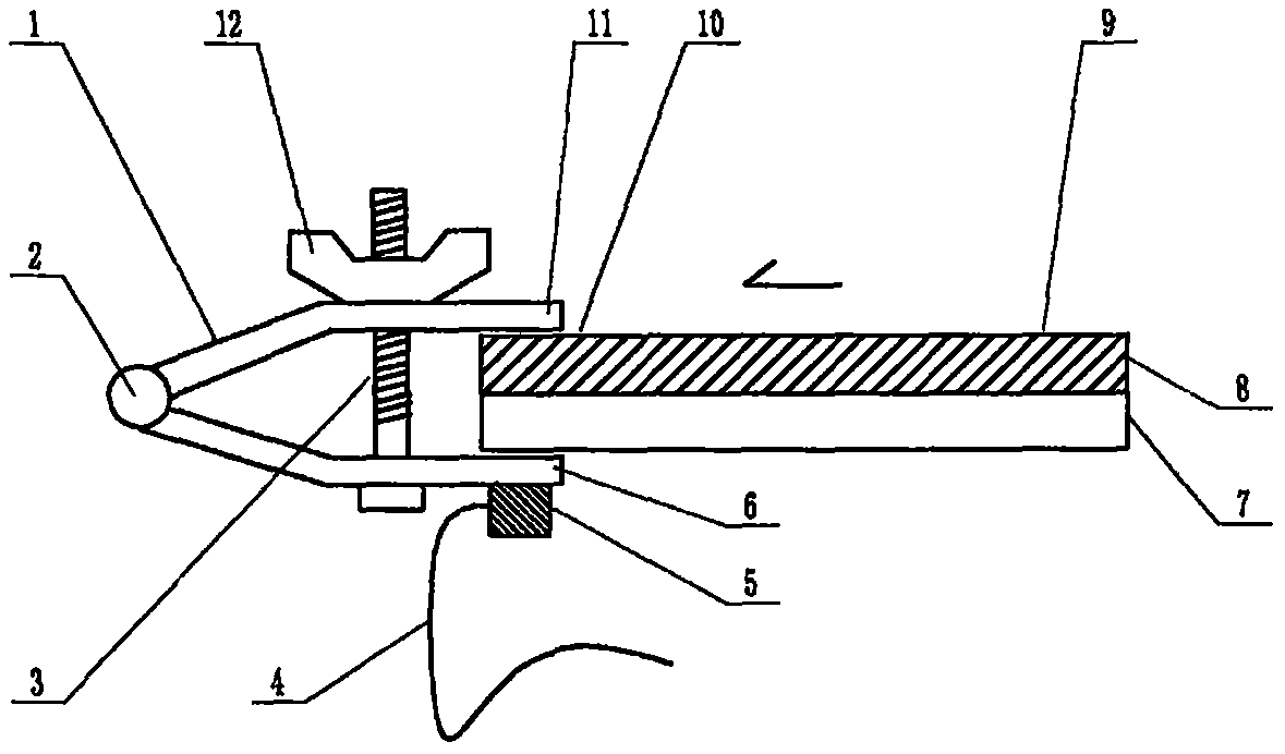
[0040] exist figure 1In the shown embodiment of the present case, the structure of the device includes a microfluidic chip, and the structure of the microfluidic chip includes a substrate 8 and a cover sheet 7 that are attached to each other. The sampling end 9 of the sample liquid flow is far away from the terminal 10 of the sample liquid flow, and the distance between the sampling end 9 and the terminal 10 is between 3 cm and 10 cm. The microfluidic chip is tested The sampling end of the sample liquid flow is provided with an injection end liquid pool, and the terminal of the sample liquid flow is provided with a terminal liquid pool, and the two ends of the pipeline in the chip are connected to the sample injection end liquid pool and the terminal liquid pool respectively. Connected, the point is that the material of the substrate 8 is polydimethylsiloxane material, and the surface of the substrate 8 is a surface in a native form. The surface in a native form means that it ...


PUM

PropertyMeasurementUnit
Thicknessaaaaaaaaaa

Abstract

The invention relates to a microfluidic chip device with polydimethylsiloxane as a substrate material and belongs to the field of analysis and testing. By using cheap and easily-processable polydimethylsiloxane, namely PDMS for manufacturing a substrate of a microfluidic chip, there exist some problems. The surface of the PDMS material is strongly hydrophobic. Through targeted surface modification, the effect is hard to last. The scheme aims to solve the series of related problems. According to main points of the scheme, PDMS with primitive surface is selected as the substrate, a hinge-type fixture attached with a miniature ultrasonic transducer is manually fastened and positioned near the terminal of a sample liquid fluid of the microfluidic chip, interfacial tension is reduced by ultrasonic wave, and by PDMS's strong absorption of ultrasonic wave, ultrasonic intensity is rapidly decreased progressively in a short distance so as to form interfacial tension difference between two endsof the chip. Thereby, the sample liquid fluid is driven to flow along an originally hydrophobic capillary channel towards the terminal.

Description

technical field [0001] The invention relates to a microfluidic chip device using polydimethylsiloxane as a substrate material, belonging to the field of analysis and testing. Background technique [0002] For the overall overview of microfluidic technology itself, you can refer to the monograph "Illustrated Microfluidic Chip Laboratory" published by the famous microfluidic expert Mr. Lin Bingcheng not long ago, which has been published by Science Press. The past, present, and future prospects of fluidic technology, etc., all have detailed and long-form expositions that go deep into specific details. [0003] The fields where microfluidic chips are often applied include various analysis and detection of sample solutions containing biomacromolecules. [0004] The basic structure of a microfluidic chip includes a substrate etched with tiny liquid flow channels and a cover sheet attached to it. The tiny liquid flow channels on the substrate, before the cover sheet is assembled,...

Claims


Application Information

Patent Timeline
IPC IPC(8): B01L3/00
CPCB01L3/5027B01L3/50273B01L2200/027B01L2200/10B01L2300/0861B01L2300/0887B01L2300/12B01L2300/166
Inventor 洪小女
Owner 洪小女
Why Eureka
Try Eureka