Stage structure of three-dimensional memory and formation method of stage structure

A memory and step technology, which is applied in the manufacture of electrical solid-state devices, semiconductor devices, semiconductor/solid-state devices, etc., can solve the problems of complex process, large volume of 3D memory, high production cost of 3D memory, etc., to reduce production cost and volume Effect

Active Publication Date: 2018-02-02
YANGTZE MEMORY TECH CO LTD
View PDF3 Cites 12 Cited by
  • Summary
  • Abstract
  • Description
  • Claims
  • Application Information

AI Technical Summary

Problems solved by technology

Existing stepped structures are usually formed by depositing an oxynitride layer and combining an etching process; the thickness of each layer of the oxynitride layer is usually about 10 microns, and with the demand for large storage capacity, the number of layers of the stepped structure has increased. Doing more and more makes the virtual area (Dummy Staircase) that is not used to place real steps larger and larger, and the volume of the three-dimensional memory is also larger and larger; and in the etching process, each etching forms a layer of steps It is necessary to use a mask plate, which makes the manufacturing cost of the three-dimensional memory very high; in addition, in the existing step structure manufacturing process, usually more than two connection holes are formed on each step according to the requirements, and the process is complicated

Method used


Image

  • Stage structure of three-dimensional memory and formation method of stage structure
  • Stage structure of three-dimensional memory and formation method of stage structure
  • Stage structure of three-dimensional memory and formation method of stage structure

Examples


Embodiment 1

[0032] According to an embodiment of the present invention, a step structure in a three-dimensional memory is provided, such as figure 1 and figure 2 shown, including:

[0033] Substrate;

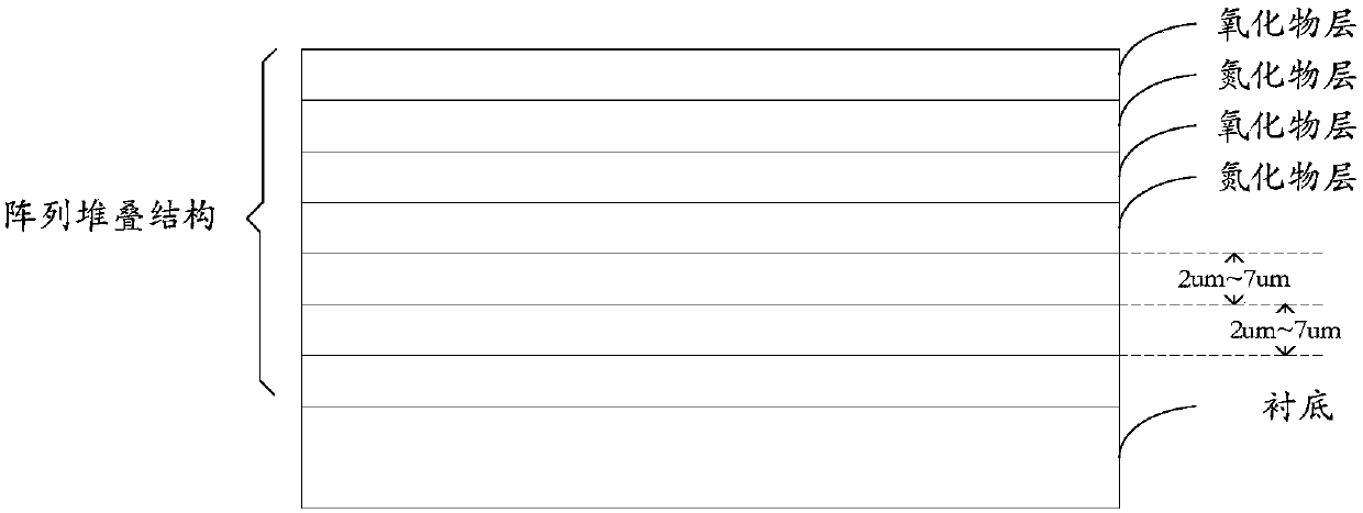
[0034] An array stack structure on a substrate;

[0035] The array stack structure includes multiple layers of nitride layers and oxide layers deposited alternately with a preset thickness, and the nitride layer is located between adjacent oxide layers;

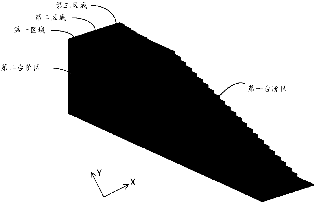
[0036] A step structure with three regions and multi-layer steps is formed by performing three etching processes in the Y direction and multiple times in the X direction on the array stack structure through a mask plate.

[0037] Wherein, the substrate is preferably a silicon substrate;

[0038] It should be noted that the number of nitride layers and oxide layers in the array stack structure depends on requirements, figure 2 For example only.

[0039] According to an embodiment of the present invention, the predetermined thickness...

Embodiment 2

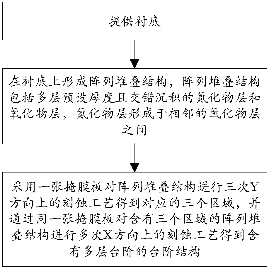
[0046] According to an embodiment of the present invention, a method for forming a step structure suitable for the three-dimensional memory described in Embodiment 1 is provided, such as image 3 shown, including:

[0047] provide the substrate;

[0048] An array stack structure is formed on the substrate, the array stack structure includes multiple layers of nitride layers and oxide layers deposited alternately with a preset thickness, and the nitride layer is formed between adjacent oxide layers;

[0049] Use a mask plate to etch the array stack structure three times in the Y direction to obtain the corresponding three regions, and perform multiple times of etching in the X direction on the array stack structure containing three regions through the same mask plate The etching process obtains a stepped structure containing multiple steps.

[0050] Wherein, the substrate is preferably a silicon substrate, and the number of nitride layers and oxide layers in the array stack s...


PUM


Abstract

The invention discloses a stage structure of a three-dimensional memory and a formation method of the stage structure, and belongs to the technical field of a semiconductor. The method comprises the steps of providing a substrate; forming an array stacked structure on the substrate, wherein the array stacked structure comprises multiple layers of nitride layers and oxide layers which are depositedin a staggered manner with preset thicknesses, and the nitride layers are formed between adjacent oxide layers; and performing three times of an etching process in a Y direction on the array stackedstructure by adopting a mask plate to obtain three corresponding regions, and performing multiple times of the etching process in an X direction on the array stacked structure comprising the three regions by adopting the same mask plate to obtain the stage structure comprising multiple layers of stages. By virtue of the formation method, on the basis that the capacity and processing reliability ofthe three-dimensional storage are ensured, the volume of the three-dimensional memory is reduced, and the manufacturing cost of the three-dimensional memory is greatly lowered.

Description

technical field [0001] The invention relates to the technical field of semiconductors, in particular to a step structure of a three-dimensional memory and a forming method thereof. Background technique [0002] With the continuous development of the demand for integration and storage capacity, three-dimensional memory emerges as the times require. Three-dimensional memory is a new type of product based on planar memory. Its main feature is to convert the planar structure into a three-dimensional structure to greatly save the area of ​​the silicon chip. Therefore, the step structure is one of the important components of the three-dimensional memory. Existing stepped structures are usually formed by depositing an oxynitride layer and combining an etching process; the thickness of each layer of the oxynitride layer is usually about 10 microns, and with the demand for large storage capacity, the number of layers of the stepped structure has increased. Doing more and more makes ...

Claims


Application Information

Patent Timeline
Patent Type & Authority Applications(China)
IPC IPC(8): H01L21/311H01L27/11551H01L27/11578
CPCH01L21/31144H10B41/20H10B43/20
Inventor 刘丹吕震宇李勇娜宋立东何洪楷冯乃柏谭经纶杨伟毅
Owner YANGTZE MEMORY TECH CO LTD
Why Eureka
Try Eureka