Conductive Structure And Manufacturing Method Therefor
A manufacturing method and structure technology, applied in the direction of conductive pattern formation, conductive pattern layout details, printed circuits, etc., can solve problems such as glare, and achieve the effects of reduced connection resistance, excellent physical durability, and excellent visibility
- Summary
- Abstract
- Description
- Claims
- Application Information
AI Technical Summary
Problems solved by technology
Method used
Image
Examples
Embodiment Construction
[0029] In this specification, it will be understood that when an element is referred to as being "on" another element, it can be directly on the other element, or intervening elements may also be present.
[0030] Throughout the specification, unless expressly stated otherwise, the word "comprising" should be understood to mean the inclusion of stated elements, but not the exclusion of any other elements.
[0031] The term "conductivity" in this specification refers to electrical conductivity.
[0032] In addition, in this specification, "reflectance" means light reflectance, "refractive index" means light refraction, and "absorption rate" means light absorption.
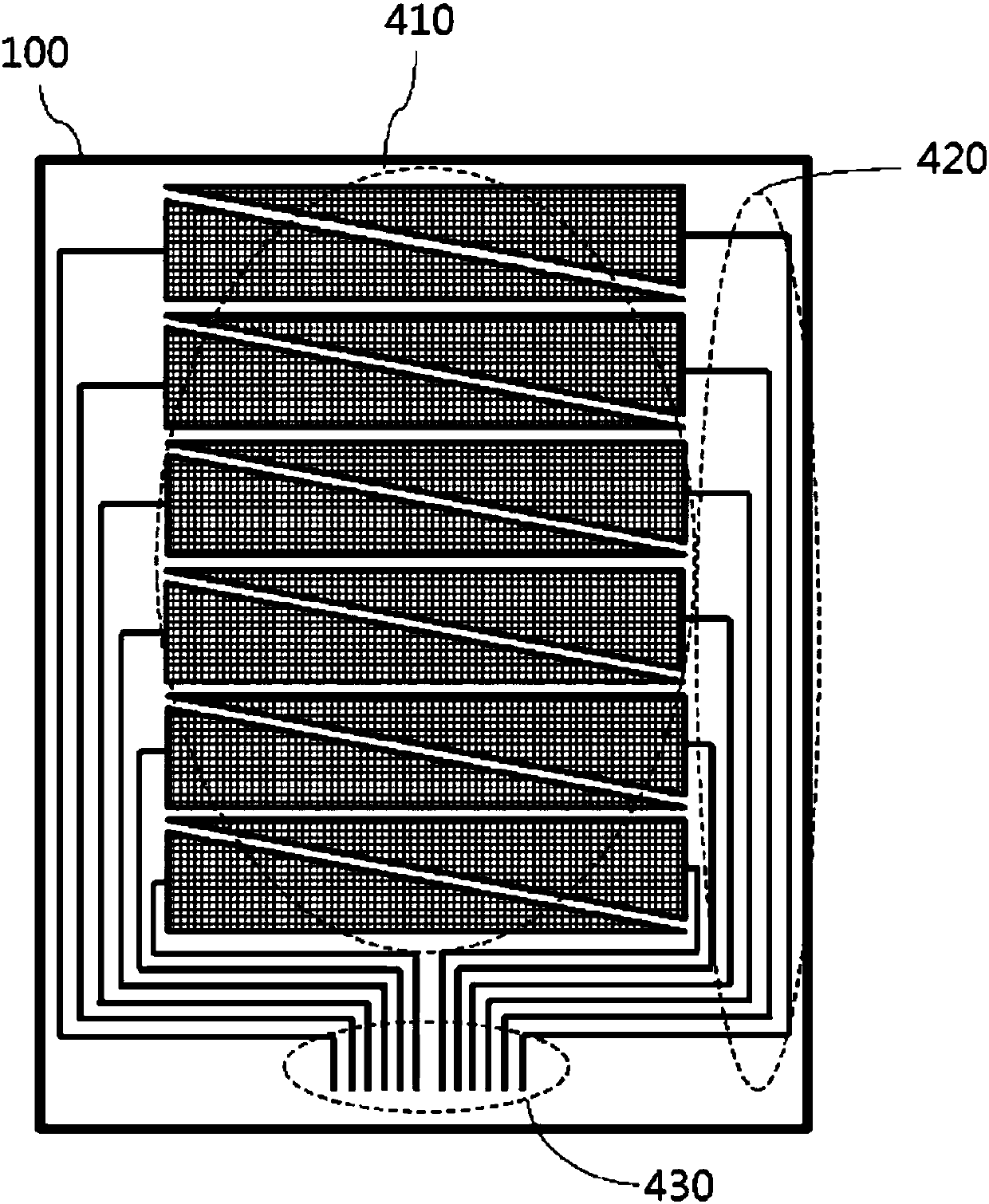
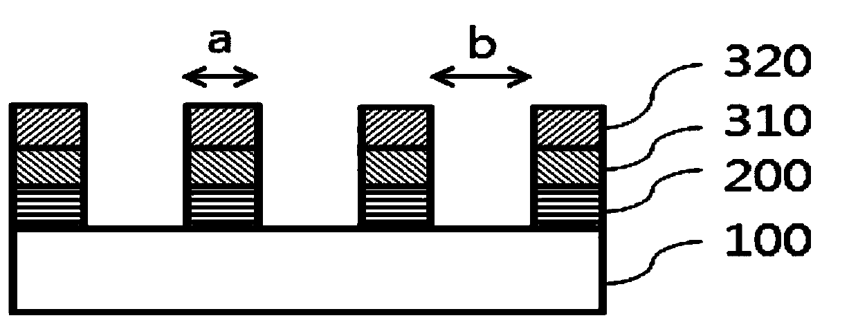
[0033] The inventors of the present invention have found the following problem. When forming the light-reducing reflection layer instead of the ITO film to prevent the glare phenomenon of the metal mesh, the light-reducing reflection layer is provided on the wire constituting the pad portion connected to the flexibl...
PUM
 Abstract
Description
Claims
Application Information


