Thickness measurement device for production of silicon chip

A thickness measurement and thickness detection technology, applied in the direction of mechanical thickness measurement, mechanical roughness/irregularity measurement, etc., can solve the problems of complicated operation and unreliable fixing.

Inactive Publication Date: 2018-02-09
周航洋
View PDF3 Cites 8 Cited by
  • Summary
  • Abstract
  • Description
  • Claims
  • Application Information

AI Technical Summary

Problems solved by technology

[0006] In order to overcome the shortcomings of the existing silicon wafer thickness measuring device that can only detect the thickness of it, and it is not fixed securely and the operation is complicated during the detection process, the technical problem to be solved by the present invention is to provide a Thickness measuring device for silicon wafer production with flatness detection, firm fixation, and simple operation

Method used


Image

  • Thickness measurement device for production of silicon chip
  • Thickness measurement device for production of silicon chip
  • Thickness measurement device for production of silicon chip

Examples


Embodiment 1

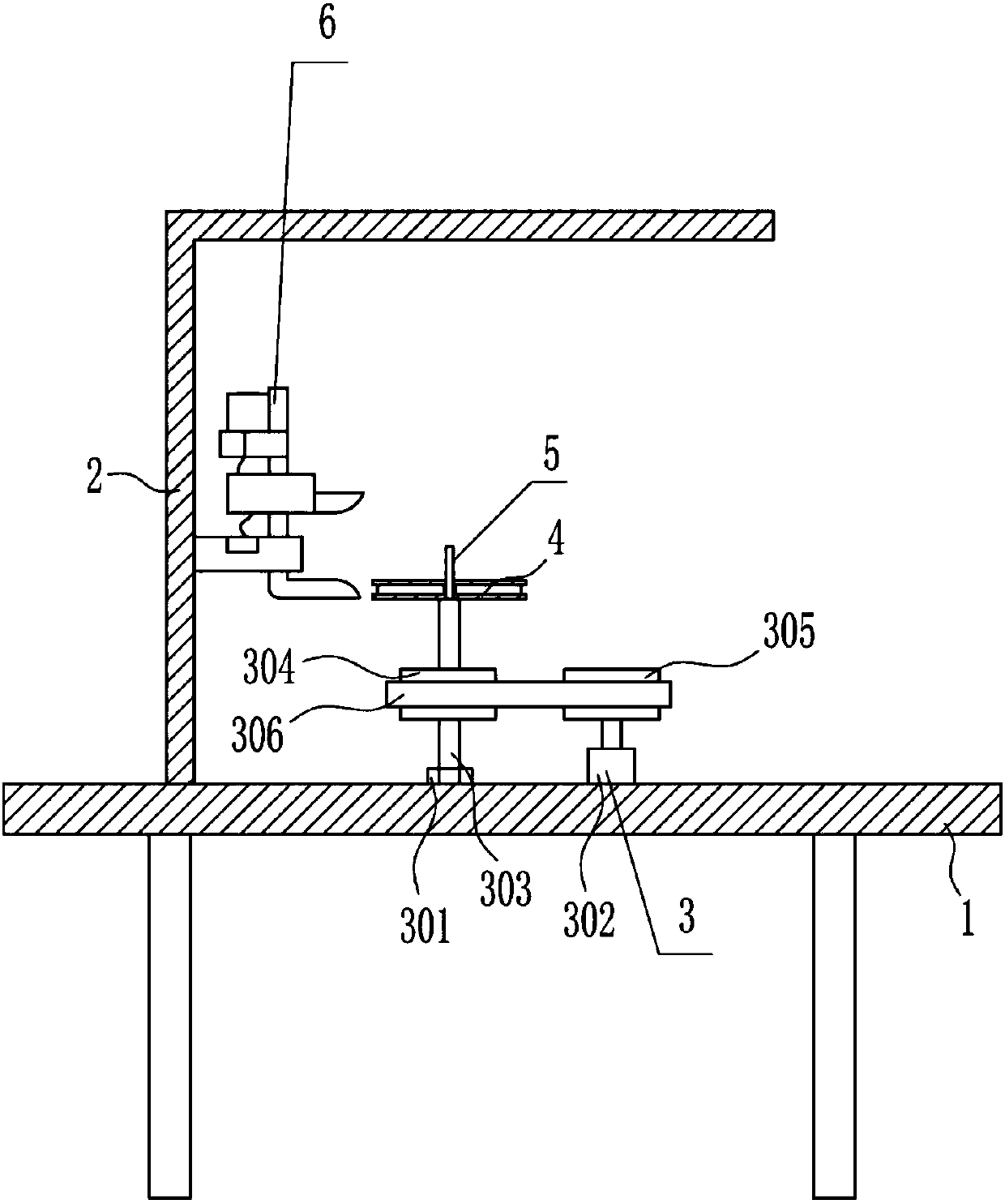
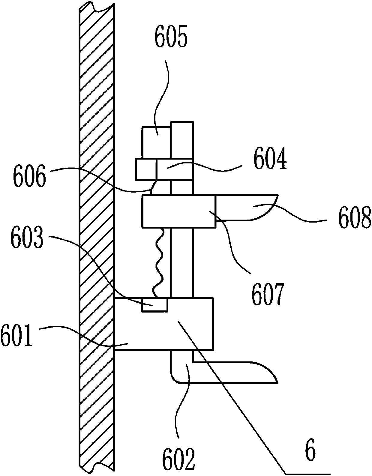
[0039] A thickness measuring device for silicon wafer production, such as Figure 1-8 As shown, it includes a workbench 1, a 7-type plate 2, a rotating device 3, a circular placing plate 4, a fixing device 5 and a thickness detection device 6. The top left side of the workbench 1 is welded with a 7-type plate 2 and a 7-type plate 2 A thickness detection device 6 is provided on the left side, and a rotating device 3 is provided in the middle of the top of the workbench 1 .

Embodiment 2

[0041] A thickness measuring device for silicon wafer production, such as Figure 1-8 As shown, it includes a workbench 1, a 7-type plate 2, a rotating device 3, a circular placing plate 4, a fixing device 5 and a thickness detection device 6. The top left side of the workbench 1 is welded with a 7-type plate 2 and a 7-type plate 2 A thickness detection device 6 is provided on the left side, and a rotating device 3 is provided in the middle of the top of the workbench 1 .

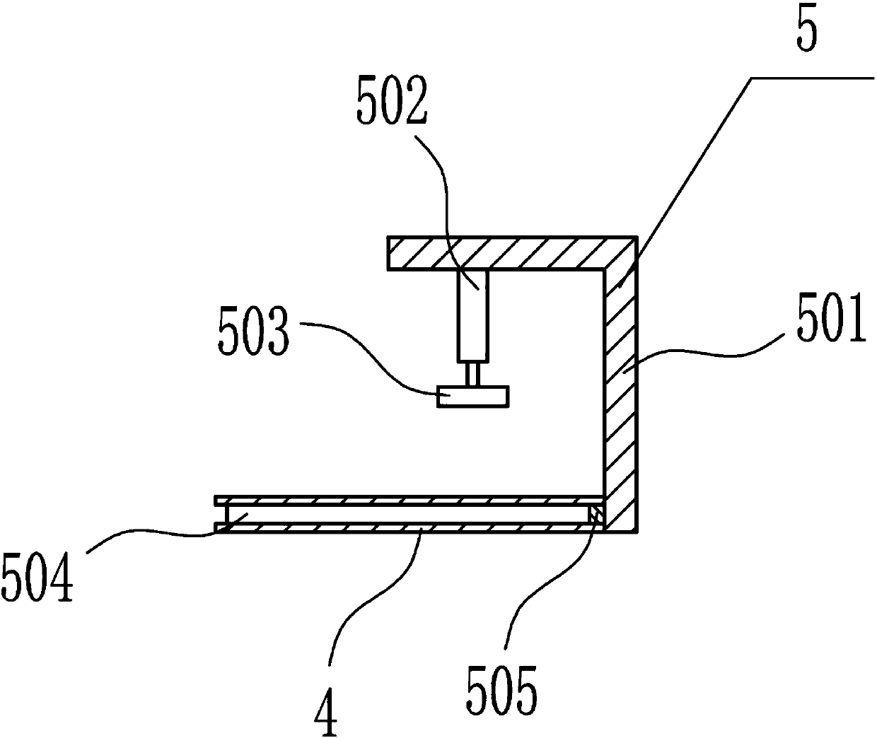
[0042] The fixing device 5 includes a 7-type fixing plate 501, a first cylinder 502, a rubber block 503 and a slide block 505. The circular placement plate 4 is provided with an annular chute 504, and the sliding type on the annular chute 504 is provided with a slide block 505. A 7-type fixed plate 501 is connected to the front of the slide block 505, and the inner bottom of the 7-type fixed plate 501 is connected with a first cylinder 502 by bolts, and a rubber block 503 is connected on the expansion rod o...

Embodiment 3

[0044] A thickness measuring device for silicon wafer production, such as Figure 1-8 As shown, it includes a workbench 1, a 7-type plate 2, a rotating device 3, a circular placing plate 4, a fixing device 5 and a thickness detection device 6. The top left side of the workbench 1 is welded with a 7-type plate 2 and a 7-type plate 2 A thickness detection device 6 is provided on the left side, and a rotating device 3 is provided in the middle of the top of the workbench 1 .

[0045] The fixing device 5 includes a 7-type fixing plate 501, a first cylinder 502, a rubber block 503 and a slide block 505. The circular placement plate 4 is provided with an annular chute 504, and the sliding type on the annular chute 504 is provided with a slide block 505. A 7-type fixed plate 501 is connected to the front of the slide block 505, and the inner bottom of the 7-type fixed plate 501 is connected with a first cylinder 502 by bolts, and a rubber block 503 is connected on the expansion rod o...


PUM


Abstract

The invention relates to a device for measuring the thickness of a silicon chip, and especially relates to a thickness measurement device for the production of the silicon chip. A technical problem tobe solved by the invention is to provide the thickness measurement device which can be used for the flatness detection of the silicon chip, is firm in fixing, and is easy to operate. In order to solve the above problem, the device provided by the invention comprises a workbench. The left side of the top of the workbench is provided with a 7-shaped plate through welding, and the left side of the 7-shaped plate is provided with a thickness detection apparatus. The center of the top of the workbench is provided with a rotating apparatus, and a rotating part on the rotating apparatus is connectedwith a circular placement plate, wherein the circular placement plate is provided with a fixing apparatus. According to the invention, the thickness detection apparatus is used for the thickness detection of the silicon chip, and a flatness detection device is used for the flatness detection of the silicon chip, thereby achieving the flatness detection of the silicon chip. The device is convenient to use, and is easy to operate.

Description

technical field [0001] The invention relates to a device for measuring the thickness of a silicon wafer, in particular to a device for measuring the thickness of a silicon wafer. Background technique [0002] On a silicon chip the size of a grain of rice, 160,000 transistors have been integrated, which is another milestone in the progress of science and technology. [0003] The silicon element with a content of 25.8% in the earth's crust provides an inexhaustible source for the production of monocrystalline silicon. Since silicon is one of the most abundant elements in the earth's crust, for products destined to enter the mass market, such as solar cells, the advantage of reserves is also one of the reasons why silicon has become the main material for photovoltaics. [0004] The existing silicon wafer thickness measuring device has the disadvantages that it can only detect the thickness, is not fixed firmly during the detection process, and is complicated to operate. Easy-...

Claims


Application Information

Patent Timeline
Patent Type & Authority Applications(China)
IPC IPC(8): G01B5/06G01B5/28
CPCG01B5/06G01B5/28
Inventor 周航洋胡瀚博夏思琪
Owner 周航洋
Why Eureka
Try Eureka