Low-defect-porous polishing pad
A polishing pad and polishing layer technology, which is applied in the direction of grinding machine tools, manufacturing tools, grinding tools, etc., can solve the problem of increasing the polishing rate
- Summary
- Abstract
- Description
- Claims
- Application Information
AI Technical Summary
Problems solved by technology
Method used
Image

Examples
example 1
[0046] This example is based on 1.5mm thick porous polyurethane polishing pad, which has 0.002m. 2 Opened vertical pores of an average pore area and a height of 0.39 mm. The polishing pad has a weight density of 0.409 g / ml. The polishing pad has an embossing groove of the size of Table 1.
[0047] Table 1
[0048] Size / slope
unit
Pad A
Pad 1
Pillow width
μM
1360×1360
1030×1030
Snap width at polished surface
μM
1200
1600
Groove depth
μM
400
580
Fluff layer (condensation) thickness
μM
530
530
Bottom pillar width
μM
2150
2100
Bottom groove width
μM
490
440
Groove taper
Spend
45
45
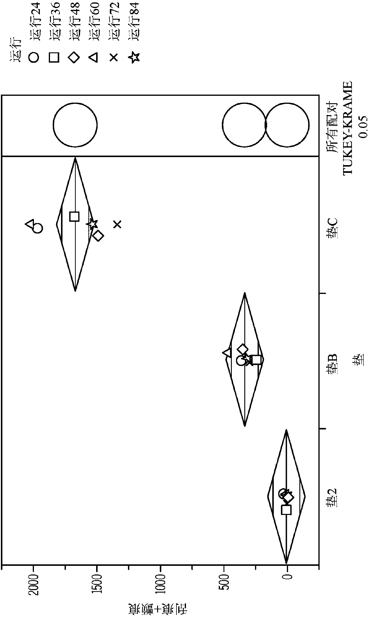
[0049] The table 1 embossed test pad was evaluated under an oxide CMP process configured for embossed depth styles. Each pad type is tested under the same process conditions. The removal rate, no uniformity% (NU%) and defects of the performance wafer are checked with the KLA-T...
example 2
[0116] The polyester felt roll has a thickness of 1.1 mM, and the weight of 334 g / m2 and the density of 0.303 g / m3. The felt is a blend of two polyester fibers that can be contracted (-55% at 70 ° C) than a ratio of contraction (-2.5% at 70 ° C). The first fiber has a weight of 2.10 Cg / 1000m, and the strength of 3.30 cn / dtex and 75% fracture elongation. The second fiber has a weight of 2.29 dtex (kg / 1000m), the strength of 2.91 c N / DTEX and 110% elongation at break. The upper surface of the felt is applied with Ag-E092 perfluorocarboxylic acid and its precursor. After the waterproof, the felt dried and burned to remove any fiber terminal protruding through the top layer of the felt.
[0117] A series of porous polishing pads are produced by the blend of thermoplastic plastics in the dimethylformamide solvent and embossed to the size of the pad 3-2 of Example 3. Table 6 provides a list of thermoplastic polyurethane components and their molar formulations. Samprene and C...
example 3
[0156] Two mats (pad 3; pad 3-1 and mat 3-2) of the commercial porous polishing pad "D" and Example 2 are embossed to different sizes. The pad 3-1 has an embossing design, wherein the width of the pillow is above the groove width at the polishing surface; and the pad 3-2 has an embossing design, wherein the groove width is more than the pillow width as measured at the polishing surface.
[0157] Table 12
[0158] Size / slope
unit
Pad D
Pad 3-1
Pad 3-2
Pillow width
μM
2750×2750
1480×1480
1135×1135
Snap width at polished surface
μM
1250
1026
1500
Groove depth
μM
450
342
480
Fluff layer (condensation) thickness
μM
720
489
489
Bottom pillar width
μM
2164
2095
Bottom groove width
μM
309
572
Groove taper
Spend
0
45
45
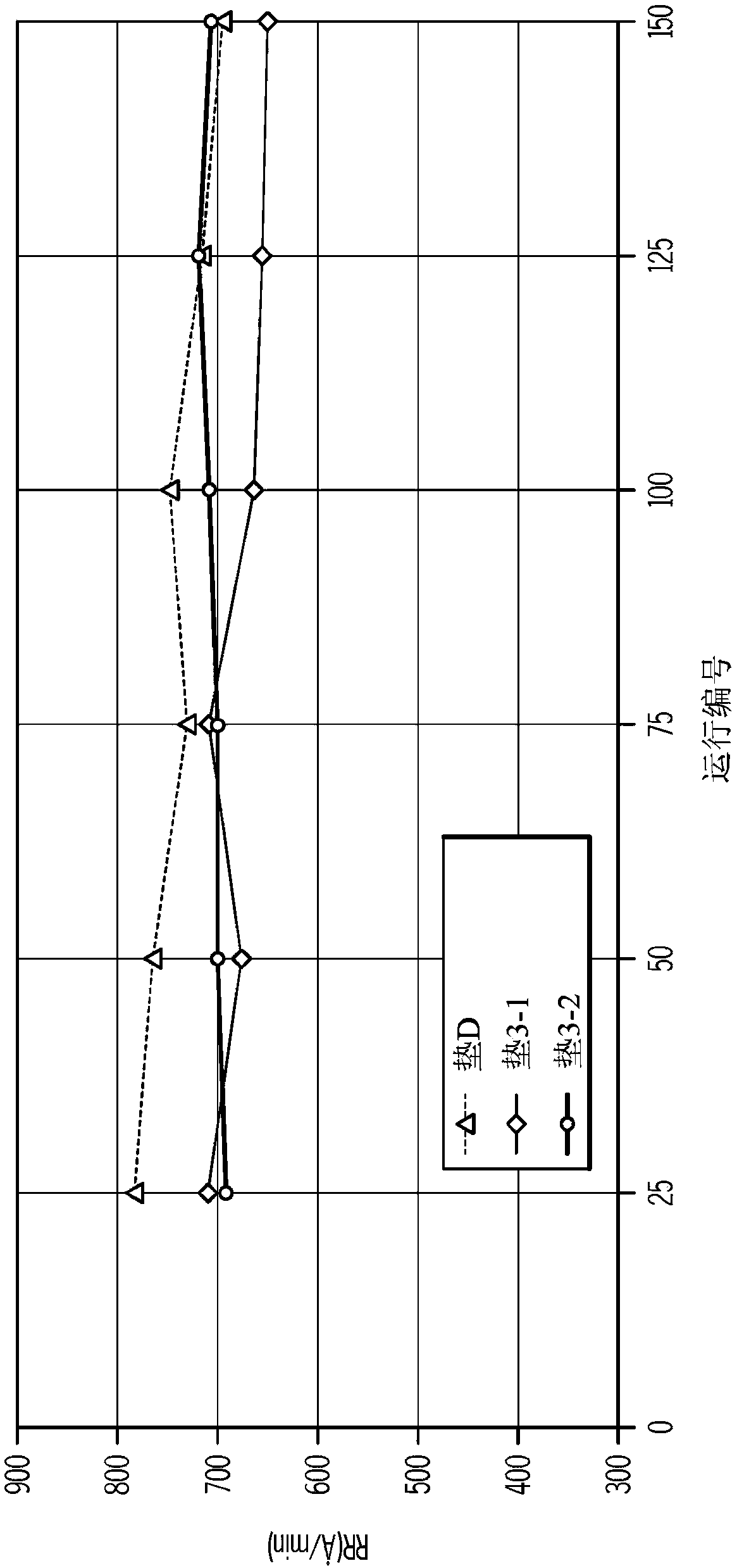
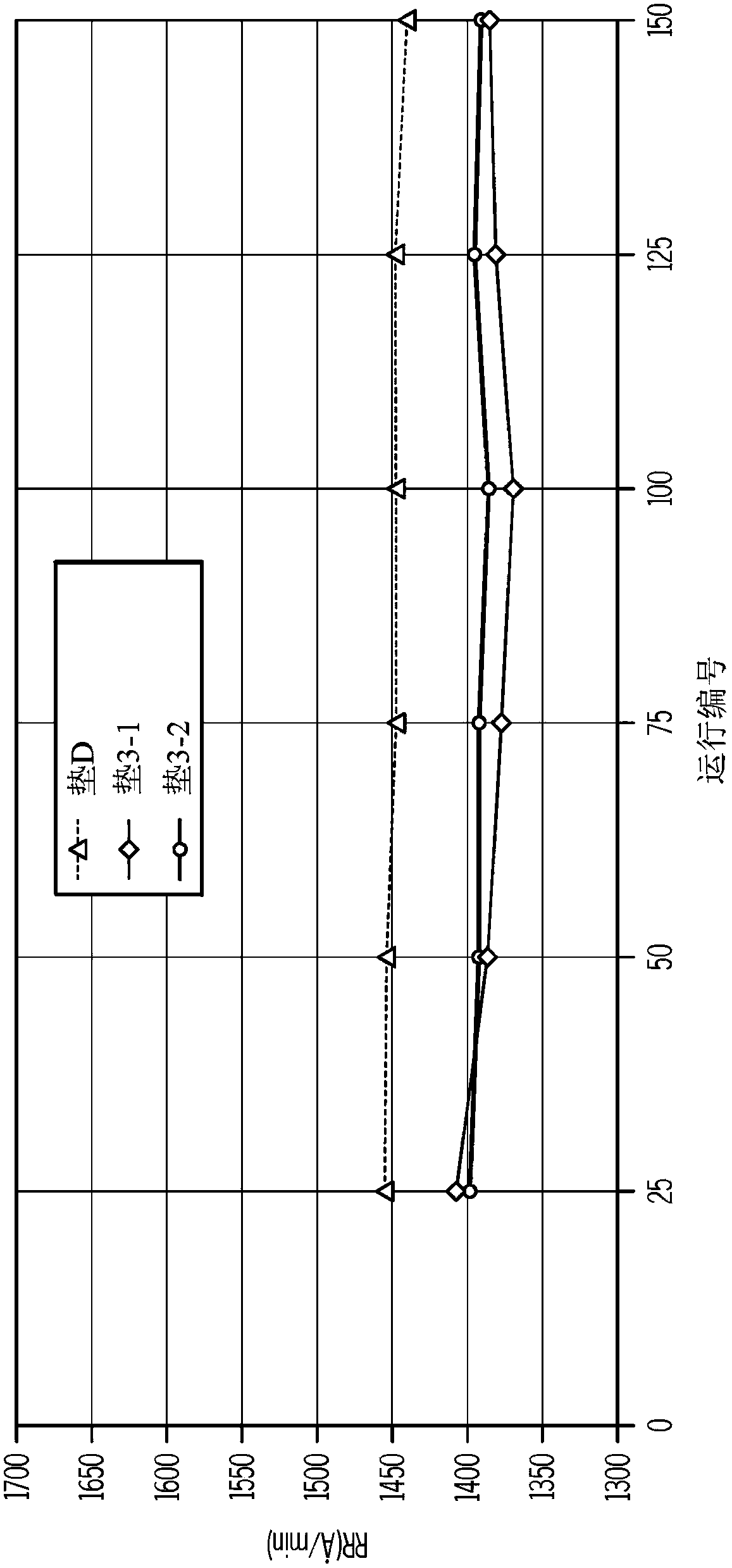
[0159] The mat was then polished under the conditions of Example 2. Table 13 and figure 2 As shown in the middle, pad...
PUM
| Property | Measurement | Unit |
|---|---|---|
| elongation | aaaaa | aaaaa |
| tensile modulus | aaaaa | aaaaa |
| tensile modulus | aaaaa | aaaaa |
Abstract
Description
Claims
Application Information
 - R&D
- Intellectual Property
- Life Sciences
- Materials
- Tech Scout
- Unparalleled Data Quality
- Higher Quality Content
- 60% Fewer Hallucinations
Browse by: Latest US Patents, China's latest patents, Technical Efficacy Thesaurus, Application Domain, Technology Topic, Popular Technical Reports.
© 2025 PatSnap. All rights reserved.Legal|Privacy policy|Modern Slavery Act Transparency Statement|Sitemap|About US| Contact US: help@patsnap.com