Production method of free nanometer columnar array for improving luminescence of OLED device

A manufacturing method and columnar technology, which is applied in the field of OLED device luminescence and micro-nano structure manufacturing, can solve the problems of high cost, high manufacturing process requirements, and complicated manufacturing process, and achieve the effects of low cost, simple process, and improved luminous brightness

Active Publication Date: 2018-02-13
HEFEI UNIV OF TECH
View PDF0 Cites 6 Cited by
  • Summary
  • Abstract
  • Description
  • Claims
  • Application Information

AI Technical Summary

Problems solved by technology

But now other types of micro-nano structures, such as micro-lenses, have complex preparation processes, require strict alignment and etching processes, have high requirements for equipment conditions and preparation processes, and are expensive

Method used


Image

  • Production method of free nanometer columnar array for improving luminescence of OLED device
  • Production method of free nanometer columnar array for improving luminescence of OLED device
  • Production method of free nanometer columnar array for improving luminescence of OLED device

Examples


Embodiment Construction

[0033] The following is a detailed description of the embodiments of the present invention. Based on the technical solution of the present invention, the present embodiment provides detailed implementation and specific operation process, but the protection scope of the present invention is not limited to the following embodiments.

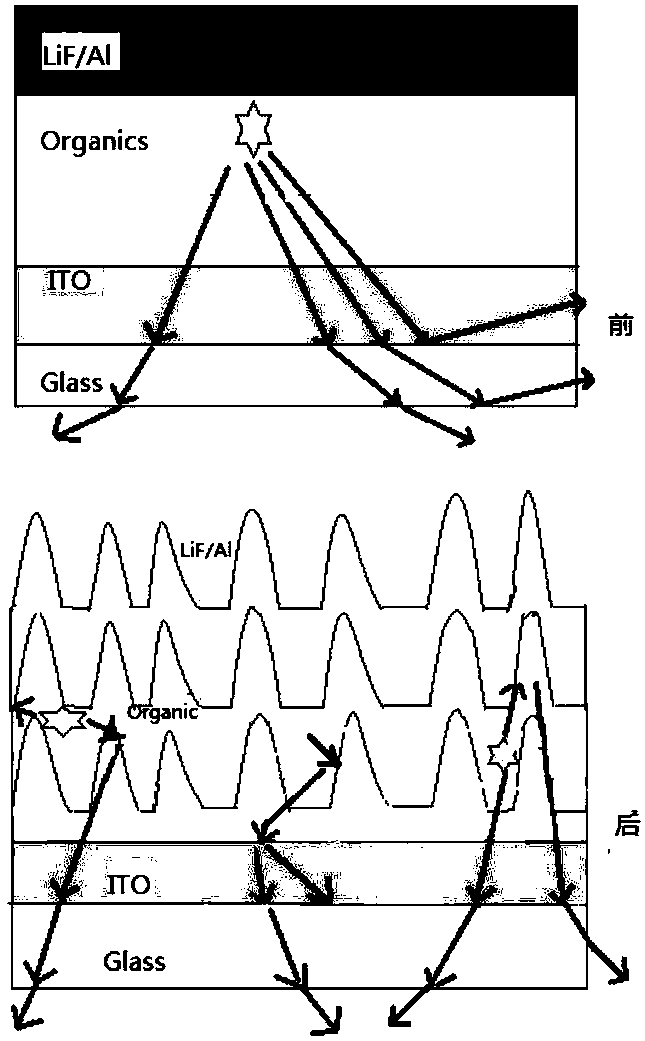
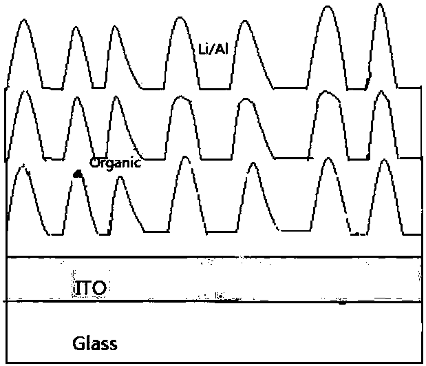
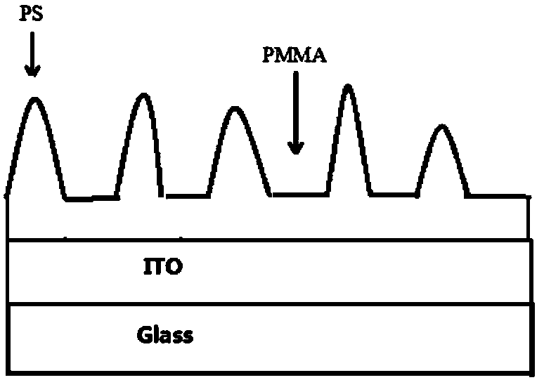
[0034] Such as figure 1 , 2 , 3, and 4, a method for making a free nanocolumn array for increasing the effective light-emitting area, comprising the following steps:

[0035] 1) ITO substrate cleaning: first rinse the ITO substrate with deionized water, then place the substrate in the laboratory ITO conductive glass cleaner with a volume concentration of 5% and deionized water for ultrasonic cleaning, and blow the cleaned substrate with nitrogen Dry, then dry on a hot table at 100°C for 10 minutes to remove residual water stains;

[0036] 2) UV ozone treatment: Place the ITO substrate cleaned in step 1) in a UV cleaning machine to remove organic ...


PUM

PropertyMeasurementUnit
diameteraaaaaaaaaa
heightaaaaaaaaaa

Abstract

The invention discloses a production method of a free nanometer columnar array for improving luminescence of an OLED device. The method comprises the steps that firstly, an ITO substrate is cleaned byusing a laboratory ITO conductive glass cleaning agent with a certain concentration and an ultraviolet light cleaning machine in sequence; then even PMMA/PS thin film is prepared by using a common technology, the ITO substrate with the PMMA/PS thin film is annealed, and a free nanometer columnar array is obtained; finally, an organic layer and an electrode layer of the OLED device are subjected to vapor deposition in sequence, and the OLED device is obtained after being packaged. According to the production method, the phase separation process of the PMMA/PS thin film is regulated and controlled, and a free nanometer columnar array structure is prepared and obtained on the ITO substrate and is applied to the OLED device; the manufacturing technology is simple, the cost is low, meanwhile,the surface area of the thin film is effectively improved, and the effective luminescence area of the device is increased; meanwhile, the light emergence angle is changed, the total reflection loss isreduced, the light emergence rate is improved, and luminescence of the OLED device is improved.

Description

technical field [0001] The invention mainly relates to the fields of OLED device luminescence and micro-nano structure fabrication, in particular to a method for fabricating a free nano-column array for enhancing OLED device luminescence. Background technique [0002] At present, the light extraction rate of OLED devices is only about 30%, and people usually use micro-nano structures to improve their light extraction efficiency. But now other types of micro-nano structures, such as micro-lenses, have complex manufacturing processes, require strict alignment and etching processes, have high requirements on equipment conditions and manufacturing processes, and are expensive. Therefore, it is necessary to develop a simple, fast and low-cost micro-nano structure preparation process to improve the light extraction rate and effective light-emitting area of ​​OLED devices, thereby enhancing its luminescence. Contents of the invention [0003] Aiming at the problems existing in t...

Claims


Application Information

Patent Timeline
Patent Type & Authority Applications(China)
IPC IPC(8): H01L51/56H01L51/52
CPCH10K50/85H10K71/00
Inventor 胡俊涛卫庆庆叶康利胡晟陆超超黄阳吕国强
Owner HEFEI UNIV OF TECH
Why Eureka
Try Eureka