
OLED device manufacturing method and corresponding OLED device

A manufacturing method and device technology, applied in the field of OLED devices, can solve the problems of poor water and oxygen barrier performance of PI substrates, small thermal expansion coefficient, shortened service life of OLEDs, etc., and achieve high feasibility and improved water and oxygen barrier performance

Inactive Publication Date: 2018-02-16
WUHAN CHINA STAR OPTOELECTRONICS SEMICON DISPLAY TECH CO LTD
View PDF5 Cites 3 Cited by
  • Summary
  • Abstract
  • Description
  • Claims
  • Application Information

AI Technical Summary

Problems solved by technology

[0004] Flexible OLED has high requirements on the performance of the substrate. In order to meet the requirements of post-process preparation and product performance, OLED substrates are often required to have properties such as flexibility, bending resistance, and high temperature resistance. At present, in the OLED industry, because polyimide (Polyimide, PI) The film itself has the advantages of high temperature resistance (up to 400 ° C), small thermal expansion coefficient (< 10), etc., and is often selected as the substrate substrate of flexible OLEDs. However, the PI substrate has poor water and oxygen resistance, so external water vapor easily passes through PI. The substrate enters the inside of the OLED device, thereby shortening the lifetime of the OLED

Method used


Image

  • OLED device manufacturing method and corresponding OLED device
  • OLED device manufacturing method and corresponding OLED device
  • OLED device manufacturing method and corresponding OLED device

Examples


Embodiment Construction

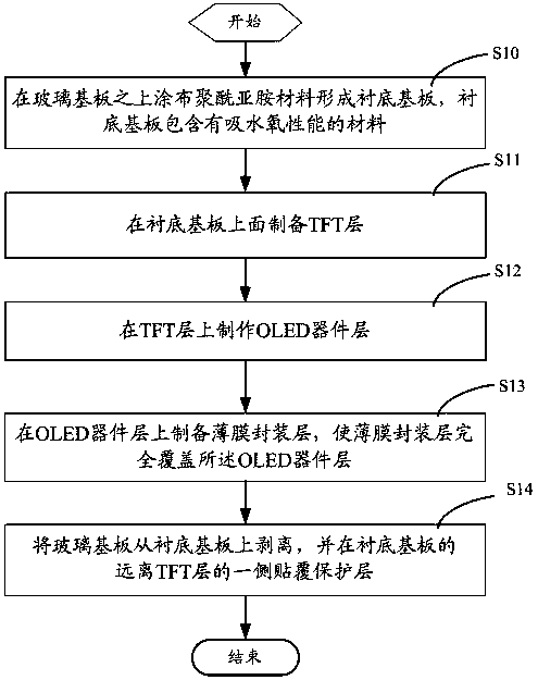
[0044] The following will clearly and completely describe the technical solutions in the embodiments of the present invention with reference to the accompanying drawings in the embodiments of the present invention. Obviously, the described embodiments are only part of the embodiments of the present invention, not all of them. Based on the embodiments of the present invention, all other embodiments obtained by persons of ordinary skill in the art without making creative efforts belong to the protection scope of the present invention.

[0045] Here, it should also be noted that, in order to avoid obscuring the present invention due to unnecessary details, only the structures and / or processing steps closely related to the solution according to the present invention are shown in the drawings, and the related Other details are not relevant to the invention.

[0046] Such as figure 1 Shown is a schematic diagram of the main process of an embodiment of a method for manufacturing an ...


PUM


Abstract

An embodiment of the invention discloses an OLED device manufacturing method, which includes the steps of coating a glass substrate with a polyimide material to form a base substrate, the base substrate comprising a material with water oxygen absorption performance; preparing a TFT layer on the base substrate; preparing an OLED device layer on the TFT layer; preparing a thin film encapsulation layer on the OLED device layer so that the thin film encapsulation layer fully covers the OLED device layer; and peeling off the glass substrate from the base substrate, and attaching a protective layeronto a far side of the base substrate away from the TFT layer. The invention also discloses a corresponding OLED device. By implementing the embodiments of the invention, the water oxygen blocking performance of a PI layer in the OLED device can be improved, and the service life of the OLED device can be increased.

Description

technical field [0001] The invention relates to the display field, in particular to a manufacturing method of an OLED device and a corresponding OLED device. Background technique [0002] Organic Light Emitting Diode (OLED) display is a promising flat panel display technology, which has self-illumination, simple structure, ultra-thin, fast response, wide viewing angle, low power consumption and flexible display. and other characteristics. At present, OLED displays are favored by major display manufacturers, and have become the third generation of displays following CRT (Cathode Ray Tube) displays and Liquid Crystal Displays (Liquid Crystal Display, LCD). [0003] However, OLED is extremely sensitive to water and oxygen. Currently commonly used OLEDs often use top emission, so the requirements for water and oxygen resistance of TFE on the surface are extremely high. At present, many patents propose how to improve the water and oxygen resistance of the upper TFE. However, fo...

Claims


Application Information

Patent Timeline
Patent Type & Authority Applications(China)
IPC IPC(8): H01L51/52H01L27/32H01L21/77
CPCH10K59/12H10K59/1201H10K59/873H10K59/874
Inventor 郭天福
Owner WUHAN CHINA STAR OPTOELECTRONICS SEMICON DISPLAY TECH CO LTD
Learn More