A three-valued static memory using word operation circuit and cnfet

A technology of static memory and arithmetic circuit, applied in static memory, digital memory information, information storage, etc., can solve the problems of increasing circuit power consumption, high power consumption of ternary static memory, large short-circuit current, etc.

Active Publication Date: 2020-05-12
NINGBO UNIV
View PDF8 Cites 0 Cited by
  • Summary
  • Abstract
  • Description
  • Claims
  • Application Information

AI Technical Summary

Problems solved by technology

[0004] figure 2 In the shown ternary static memory, 4 P-type CNFETs P1, P2, P3 and P4 and 2 N-type CNFETs N1 and N2 constitute the first ternary inverter, and 4 P-type CNFETs P5, P6, P7 and P8 and two N-type CNFET tubes N3 and N4 form the second ternary inverter, and the first ternary inverter and the second ternary inverter form a pair of cross-coupled inverters ; In the ternary static memory, when the input of the first ternary inverter is a logic value "1", the P-type CNFET tube P2 and the N-type CNFET tube N3 are simultaneously turned on and divided to obtain a logic value "1" output, At this time, a DC path is formed between the power supply Vdd connected to the first ternary inverter and the ground, resulting in a large short-circuit current; the second ternary inverter also has the same power as the first ternary inverter. The DC path problem, therefore, when the ternary static memory stores the logic value "1", there are two such DC paths, which increases the working power consumption of the circuit and makes the ternary static memory consume higher power consumption
[0005] Moreover, the above two kinds of ternary static memories all implement data storage in the form of cross-coupled inverters. Since the output terminals of the two inverters are the input terminals of each other in the cross-coupled inverter, two inverters are required when writing data. The data writing can only be completed when all terminals reach the signal inversion condition, thus increasing the data writing delay

Method used


Image

  • A three-valued static memory using word operation circuit and cnfet
  • A three-valued static memory using word operation circuit and cnfet
  • A three-valued static memory using word operation circuit and cnfet

Examples


Embodiment

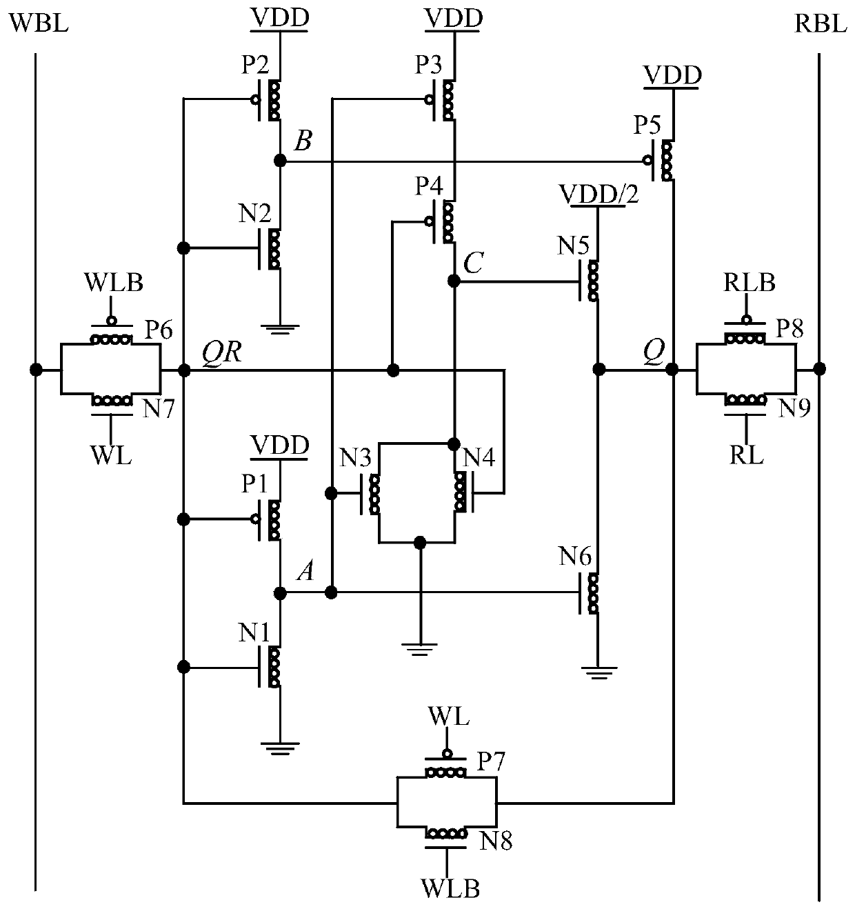
[0015] Example: such as image 3As shown, a three-valued static memory using a word operation circuit and CNFET includes a first P-type CNFET tube P1, a second P-type CNFET tube P2, a third P-type CNFET tube P3, a fourth P-type CNFET tube P4, The fifth P-type CNFET tube P5, the sixth P-type CNFET tube P6, the seventh P-type CNFET tube P7, the eighth P-type CNFET tube P8, the first N-type CNFET tube N1, the second N-type CNFET tube N2, the third N-type CNFET tube N3, fourth N-type CNFET tube N4, fifth N-type CNFET tube N5, sixth N-type CNFET tube N6, seventh N-type CNFET tube N7, eighth N-type CNFET tube N8, ninth N-type tube CNFET tube N9, write bit line WBL, read bit line RBL, write word line WL, inverted write word line WLB, read word line RL, and inverted read word line RLB; the source of the first P-type CNFET tube P1, the second P The source of the third P-type CNFET P2, the source of the third P-type CNFET P3 and the source of the fifth P-type CNFET P5 are all connected...


PUM


Abstract

The invention discloses a three-value static memory using a word operation circuit and CNFET. The three-value static memory comprises a first P-type CNFET, a second P-type CNFET, a third P-type CNFET,a fourth P-type CNFET, a fifth P-type CNFET, a sixth P-type CNFET, a seventh P-type CNFET, an eighth P-type CNFET, a first N-type CNFET, a second N-type CNFET, a third N-type CNFET, a fourth N-type CNFET, a fifth N-type CNFET, a sixth N-type CNFET, a seventh N-type CNFET, an eighth N-type CNFET, a ninth N-type CNFET, a writing bit line, a reading bit line, a writing word line, an inverted writingword line, a reading word line and an inverted reading word line. The three-value static memory has low power consumption and can reduce time delay.

Description

technical field [0001] The invention relates to a three-valued static memory, in particular to a three-valued static memory utilizing word operation circuits and CNFETs. Background technique [0002] Traditional ternary SRAMs usually store data in the form of cross-coupled inverters. At present, the circuit diagrams of two kinds of ternary static memories designed by using CNFET tubes (that is, carbon nano field effect transistors) are as follows: figure 1 and figure 2 shown. [0003] figure 1 In the three-valued static memory shown, one P-type CNFET tube P1 and two N-type CNFET tubes N1 and N2 form the first three-value inverter, and one P-type CNFET tube P2 and two N-type CNFET tubes N3 and N4 form The second ternary inverter, the first ternary inverter and the second ternary inverter constitute a pair of cross-coupled inverters; the P-type CNFET tube P3 and the N-type CNFET tube N5 are used for control data Write, P-type CNFET tube P4 and N-type CNFET tube N6 are us...

Claims


Application Information

Patent Timeline
Patent Type & Authority Patents(China)
IPC IPC(8): G11C11/417
CPCG11C11/417
Inventor 汪鹏君康耀鹏李刚张跃军
Owner NINGBO UNIV
Why Eureka
Try Eureka