Supercharge Your Innovation With Domain-Expert AI Agents!

Forming method of step structure

A step and step layer technology, applied in the direction of electrical components, electric solid devices, circuits, etc., can solve the problems of increasing the production cost of the step structure, achieve the effect of improving the process margin and reducing the production cost

Active Publication Date: 2018-02-23
YANGTZE MEMORY TECH CO LTD
View PDF9 Cites 0 Cited by
  • Summary
  • Abstract
  • Description
  • Claims
  • Application Information

AI Technical Summary

Problems solved by technology

Among them, the formation of the uppermost single-layer stepped layers in the stepped structure is formed by etching with a thicker nitride as a mask, and the

Method used


Image

  • Forming method of step structure
  • Forming method of step structure
  • Forming method of step structure

Examples


Embodiment Construction

[0042] Exemplary embodiments of the present disclosure will be described in more detail below with reference to the accompanying drawings. Although exemplary embodiments of the present disclosure are shown in the drawings, it should be understood that the present disclosure may be embodied in various forms and should not be limited by the embodiments set forth herein. Rather, these embodiments are provided for more thorough understanding of the present disclosure and to fully convey the scope of the present disclosure to those skilled in the art.

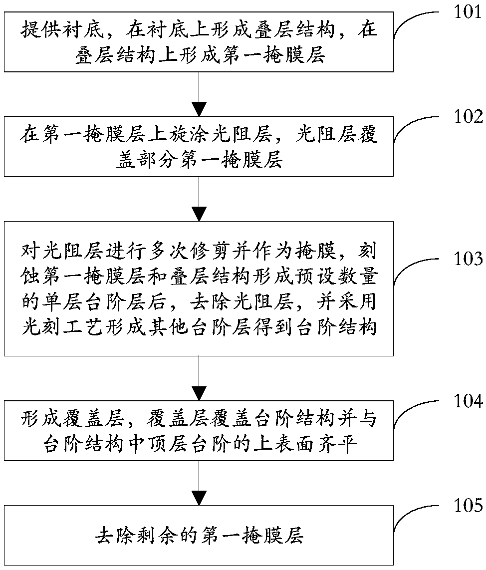
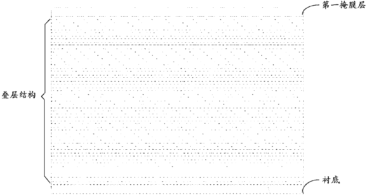
[0043] According to an embodiment of the present invention, a method for forming a stepped structure is provided, such as figure 1 shown, including:

[0044] providing a substrate, forming a laminated structure on the substrate, and forming a first mask layer on the laminated structure;

[0045] spin-coating a photoresist layer on the first mask layer, the photoresist layer covering part of the first mask layer;

[0046] Trim the...


PUM


Abstract

The invention discloses a forming method of a step structure, which belongs to the technical field of semiconductors. The method comprises the steps of providing a substrate, forming a lamination structure on the substrate, and forming a first mask layer on the lamination structure; spin coating a photoresist layer on the first mask layer, wherein the photoresist layer covers a part of the first mask layer; conducting multiple trimming on the photoresist layer, and etching the first mask layer and the lamination structure to form a single step layer, and removing the photoresist layer, and adopting photoetching process to form other step layers to form the step structure; forming a cover layer which covers the step structure and aligns with the upper surface of the top step of the step structure; removing the left first mask layer. The invention is advantageous in that a plurality of single step layers at the top of the step structure can be formed through the same mask layer, which not only improves the technology margin of chemical and mechanical grinding during the step structure forming process, but also reduces the producing cost.

Description

technical field [0001] The invention relates to the technical field of semiconductors, in particular to a method for forming a stepped structure. Background technique [0002] With the continuous development of the demand for integration and storage capacity, three-dimensional memory emerges as the times require. Three-dimensional memory is a new type of product based on planar memory. Its main feature is to convert the planar structure into a three-dimensional structure to greatly save the chip area. Therefore, the step structure is one of the important components of the three-dimensional memory. Existing step structures are usually formed by depositing oxynitride layers and combining etching processes. Among them, the formation of the uppermost multiple single-layer stepped layers in the stepped structure is formed by etching with a thicker nitride as a mask, and the formation of each single-layer stepped layer needs to use a corresponding nitride mask. film, which incre...

Claims


Application Information

Patent Timeline
IPC IPC(8): H01L27/11568H01L27/11578H01L21/28
CPCH01L29/40117H10B43/20H10B43/30
Inventor 吕震宇陈俊戴晓望朱继锋胡思平姚兰肖莉红郑阿曼鲍琨杨号号
Owner YANGTZE MEMORY TECH CO LTD
Features
  • R&D
  • Intellectual Property
  • Life Sciences
  • Materials
  • Tech Scout
  • Unparalleled Data Quality
  • Higher Quality Content
  • 60% Fewer Hallucinations
Learn More