Compensation circuit and display device

A technology for compensation circuits and display devices, applied in static indicators, instruments, etc., can solve the problems of large threshold voltage drift of pull-down switch tubes, decreased conductivity, affecting the working life of integrated gate drive circuits, etc., and achieve threshold voltage drift. , the effect of reducing the threshold voltage drift

Active Publication Date: 2018-03-06
KUSN INFOVISION OPTOELECTRONICS
View PDF8 Cites 3 Cited by
  • Summary
  • Abstract
  • Description
  • Claims
  • Application Information

AI Technical Summary

Problems solved by technology

These methods can achieve the purpose of prolonging the life of the integrated gate drive circuit to a certain extent, but because the pull-down switch tube is often under unipolar (positive voltage) bias, it will be subjected to a long period of positive DC voltage stress or Pulse voltage stress, the threshold voltage drift of the pull-down switch tube is still very large after a long time of work, and the conductivity will decline, which will seriously affect the working life of the integrated gate drive circuit

Method used


Image

  • Compensation circuit and display device
  • Compensation circuit and display device
  • Compensation circuit and display device

Examples


Embodiment Construction

[0024] Hereinafter, the present invention will be described in more detail with reference to the accompanying drawings. In the various figures, identical elements are indicated with similar reference numerals. For the sake of clarity, various parts in the drawings have not been drawn to scale. In addition, the drawing is not drawn except for the lead-out lines corresponding to the driving electrodes and the sensing electrodes, and some well-known parts may not be shown.

[0025] In the following, many specific details of the present invention are described, such as device structures, materials, dimensions, processing techniques and techniques, for a clearer understanding of the present invention. However, the invention may be practiced without these specific details, as will be understood by those skilled in the art.

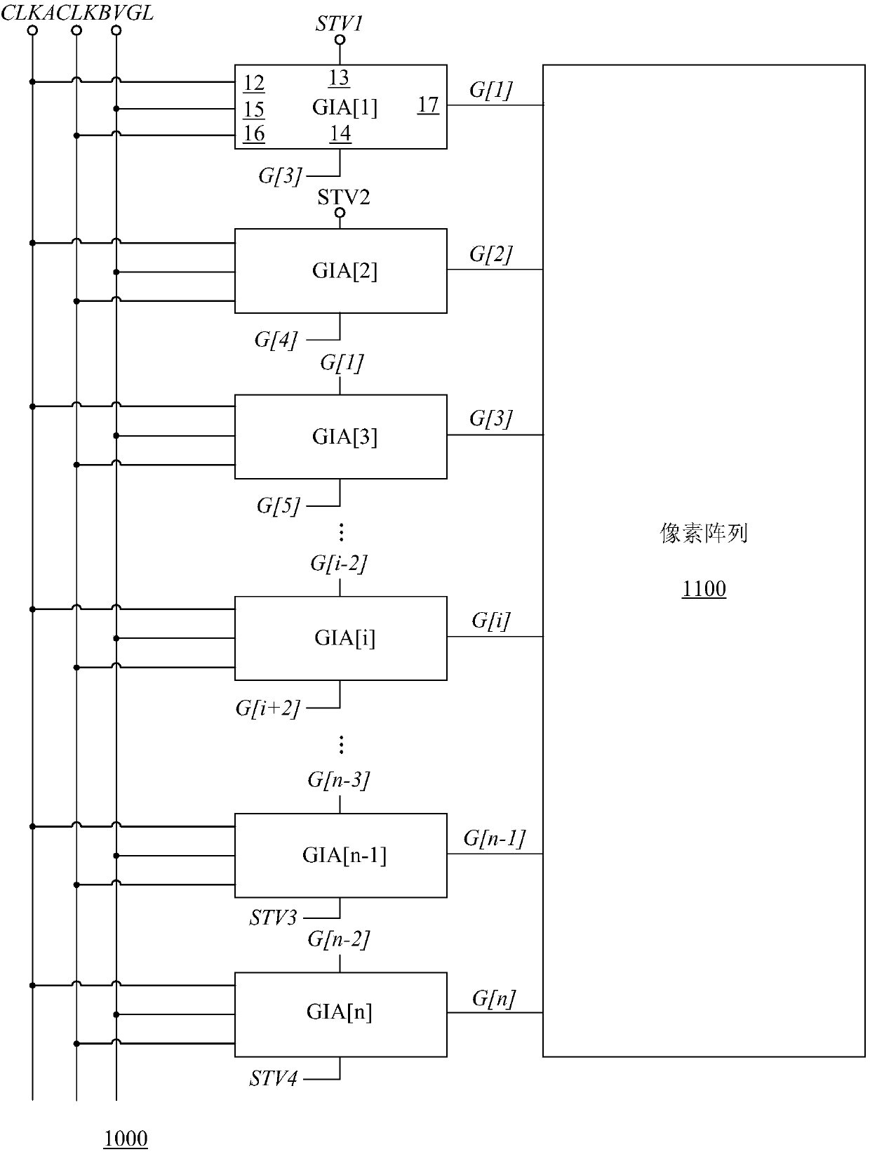
[0026] figure 1 A schematic diagram of a prior art integrated gate drive display panel is shown.

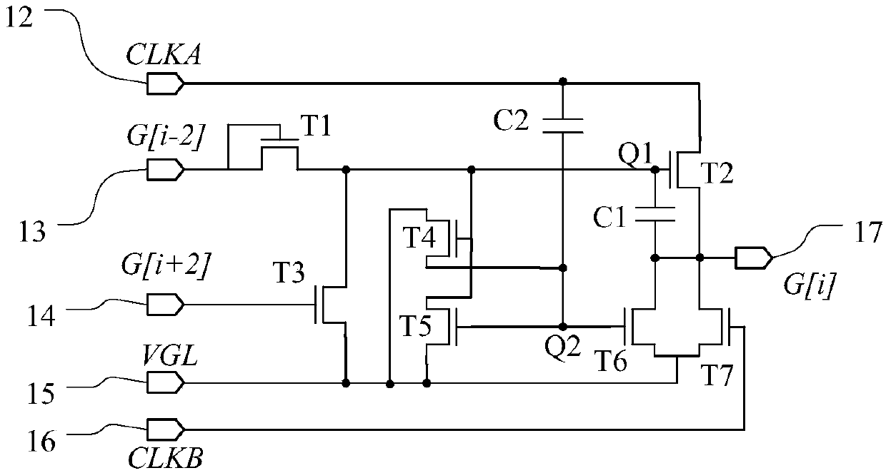
[0027] Such as figure 1 As shown, the integrated gate dr...


PUM


Abstract

The invention discloses a compensation circuit and a display device. The compensation circuit comprises a first switching tube receiving a first reference voltage, a second switching tube receiving asecond reference voltage, a pre-charging unit, a charging unit and a pull-down unit. A second access terminal of the first switching tube is connected with a second access terminal of the second switching tube to provide an output signal; the first switching tube and the second switching tube are in conduction alternately with frame switching; and phases of the first reference voltage and the second reference voltage are opposite. The pre-charging unit enables one of the first switching tube and the second switching tube to be in conduction according to a pre-stage gate drive signal; the charging unit maintains the conduction or turning-off state of the first switching tube or the second switching tube according to a local-stage gate drive signal; and the pull-down unit controls the firstswitching tube and the second switching tube according to a post-stage gate drive signal. Because transistors in the compensation circuit work alternately, the threshold voltage drifts of the transistors can be reduced and recovery of the threshold voltage drifts of the transistors is realized.

Description

technical field [0001] The present invention relates to the field of display technology, in particular to a compensation circuit and a display device. Background technique [0002] A liquid crystal display device is a display device that uses the phenomenon that the alignment direction of liquid crystal molecules changes under the action of an electric field to change the light transmittance of a light source. Due to the advantages of good display quality, small size and low power consumption, liquid crystal display devices have been widely used in mobile terminals such as mobile phones and large-sized display panels such as flat-panel televisions. Most of the liquid crystal displays currently on the market are projection type liquid crystal displays, which include a liquid crystal panel and a backlight module. The working principle of the liquid crystal panel is to place liquid crystal molecules between two parallel glass substrates, and apply a driving voltage on the two ...

Claims


Application Information

Patent Timeline
Patent Type & Authority Applications(China)
IPC IPC(8): G09G3/36
CPCG09G3/36G09G3/3677G09G3/3696
Inventor 张军李森龙吕晶张好好
Owner KUSN INFOVISION OPTOELECTRONICS
Why Eureka
Try Eureka