A wide-bandgap semiconductor lateral superjunction double-diffused transistor with multi-ring electric field modulation substrate

A semiconductor and wide bandgap technology, applied in the field of lateral superjunction double-diffused metal oxide semiconductor field effect transistors, can solve the problems of uneven distribution of surface electric field, substrate-assisted depletion SAD, etc. Effects of optimizing, eliminating substrate-assisted depletion issues

Active Publication Date: 2021-06-18
XIDIAN UNIV
View PDF7 Cites 0 Cited by
  • Summary
  • Abstract
  • Description
  • Claims
  • Application Information

AI Technical Summary

Problems solved by technology

However, there are three problems in the super junction applied to LDMOS: 1) The P-type substrate of N-channel LDMOS assists in depleting the N-type region of the super junction, resulting in substrate-assisted depletion (SAD) Problem; 2) The traditional SJ-LDMOS only forms electric field modulation between the N region and the P region of the super junction, but there is no electric field modulation on the surface; 3) Although the SJ-LDMOS that eliminates the substrate-assisted depletion can completely deplete the drift region However, due to the influence of the longitudinal electric field, the surface electric field distribution is not uniform

Method used


Image

  • A wide-bandgap semiconductor lateral superjunction double-diffused transistor with multi-ring electric field modulation substrate
  • A wide-bandgap semiconductor lateral superjunction double-diffused transistor with multi-ring electric field modulation substrate

Examples


Embodiment Construction

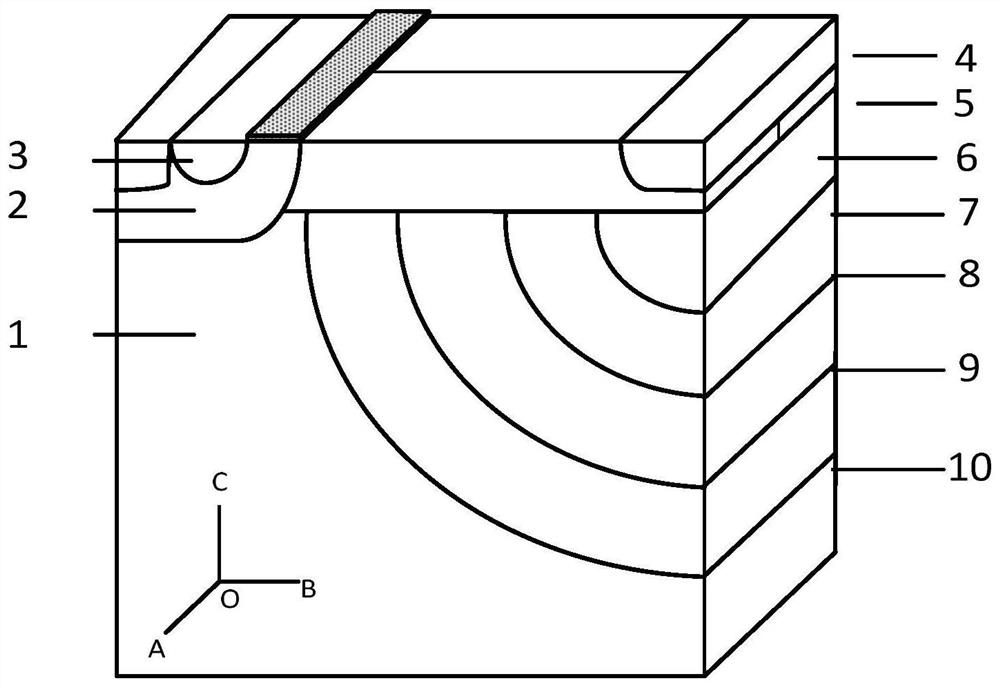
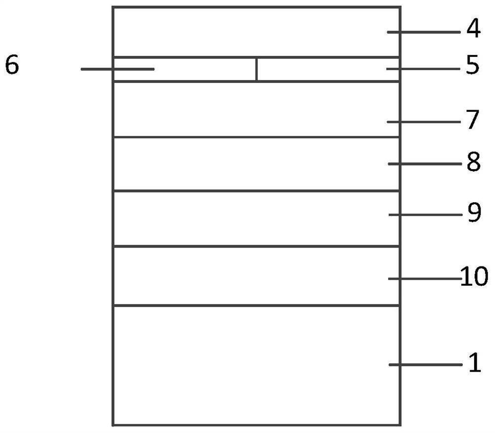
[0038] Such as figure 1 and figure 2 A wide-bandgap semiconductor lateral superjunction double-diffused transistor with a multi-ring electric field modulation substrate:

[0039] Wide bandgap semiconductor material substrate 1, the doping concentration is the concentration of general wide bandgap semiconductor material, the typical value is 1×10 13 cm -3 ~1×10 15 cm -3 ;

[0040] The base region 2 located on the surface of the wide bandgap semiconductor substrate;

[0041] Implant N-columns and P-columns on the wide bandgap semiconductor substrate from the edge of the base region, and arrange them alternately to form superjunction (SuperJunction) drift regions 5 and 6;

[0042] a source region 3 located on the surface of the base region;

[0043] The drain region 4 located on the surface of the super junction drift region;

[0044] A multi-ring electric field modulation structure located under the superjunction drift region;

[0045] Specifically:

[0046] The rings...


PUM


Abstract

The invention discloses a wide-bandgap semiconductor lateral superjunction double-diffusion transistor with a multi-ring electric field modulation substrate. The substrate under the drift region in this structure is a charge compensation polyring structure. The multi-ring charge compensation of the substrate can expand the vertical space charge region of the lateral double-diffused metal oxide semiconductor field effect transistor. The substrate-assisted depletion problem existing in the lateral superjunction uses the electric field modulation effect to simultaneously modulate the surface lateral electric field and the bulk longitudinal electric field, so that the surface lateral electric field and the bulk longitudinal electric field are simultaneously optimized. This structure not only breaks through the breakdown voltage saturation problem of the lateral double-diffused transistor due to the limited vertical withstand voltage, but also eliminates the problem of substrate-assisted depletion in the superjunction, so that the surface lateral electric field and the body vertical electric field are simultaneously optimized. , greatly increasing the breakdown voltage of the device.

Description

technical field [0001] The invention relates to the technical field of semiconductor power devices, in particular to a lateral superjunction double-diffused metal oxide semiconductor field effect transistor. Background technique [0002] Lateral Double-diffused MOSFET (LDMOS) has the advantages of easy integration, good thermal stability, good frequency stability, low power consumption, multi-subconduction, small power drive, and switching speed Advanced advantages are at the heart of smart power circuits and high-voltage devices. However, due to the limitations of the first two generations of semiconductor materials represented by Si and GaAs, the third generation of wide-bandgap semiconductor materials has developed rapidly because of its excellent performance. Wide bandgap semiconductor materials have the characteristics of large bandgap width, high electron drift saturation velocity, small dielectric constant, and good electrical conductivity. Their superior properties ...

Claims


Application Information

Patent Timeline
Patent Type & Authority Patents(China)
IPC IPC(8): H01L29/06H01L29/78
CPCH01L29/0634H01L29/0684H01L29/7816
Inventor 段宝兴杨银堂董自明
Owner XIDIAN UNIV
Why Eureka
Try Eureka