Transverse and longitudinal electric field simultaneously optimized wide-bandgap semiconductor transverse superjunction double-diffused transistor

A semiconductor and wide-bandgap technology, applied in the field of lateral superjunction double-diffused transistors, can solve the problems of substrate-assisted depletion, limited effect of lateral electric field optimization, and uneven surface electric field distribution

Inactive Publication Date: 2018-01-26
XIDIAN UNIV
View PDF3 Cites 1 Cited by
  • Summary
  • Abstract
  • Description
  • Claims
  • Application Information

AI Technical Summary

Problems solved by technology

However, there are three problems in the super junction applied to LDMOS: 1) The P-type substrate of N-channel LDMOS assists in depleting the N-type region of the superjunction, which brings about the problem of substrate-assisted depletion (SAD) ; 2) Traditional SJ-LDMOS only forms electric field modulation between the N region and P region of the super junction, but there is no electric field modulation on the surface; 3) SJ-LDMOS that eliminates substrate-assisted depletion can completely deplete the drift region , but due to the influence of the longitudinal electric field, the surface electric field distribution is not uniform
[0006] The above two schemes are actually optimized for the vertical electric field of the device, but the optimization effect for the horizontal electric field is very limited

Method used


Image

  • Transverse and longitudinal electric field simultaneously optimized wide-bandgap semiconductor transverse superjunction double-diffused transistor
  • Transverse and longitudinal electric field simultaneously optimized wide-bandgap semiconductor transverse superjunction double-diffused transistor
  • Transverse and longitudinal electric field simultaneously optimized wide-bandgap semiconductor transverse superjunction double-diffused transistor

Examples


Embodiment Construction

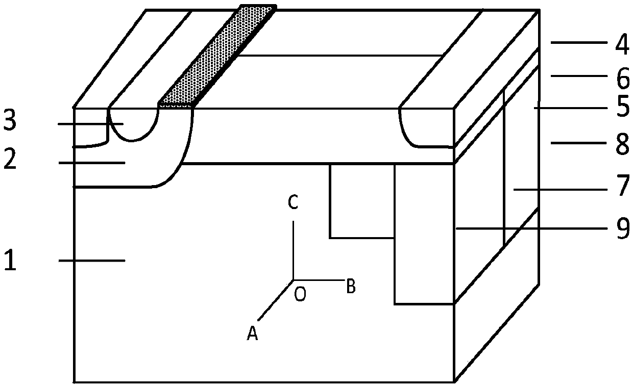
[0041] Such as figure 1 , figure 2 and image 3 Shown is a horizontal superjunction double-diffused transistor with horizontal and vertical electric fields and optimized wide bandgap semiconductor:

[0042] Wide bandgap semiconductor material substrate 1, the doping concentration is the concentration of general wide bandgap semiconductor single crystal material, the typical value is 1×10 13 cm -3 ~1×10 15 cm -3 ;

[0043] The base region 2 located on the surface of the wide bandgap semiconductor material substrate;

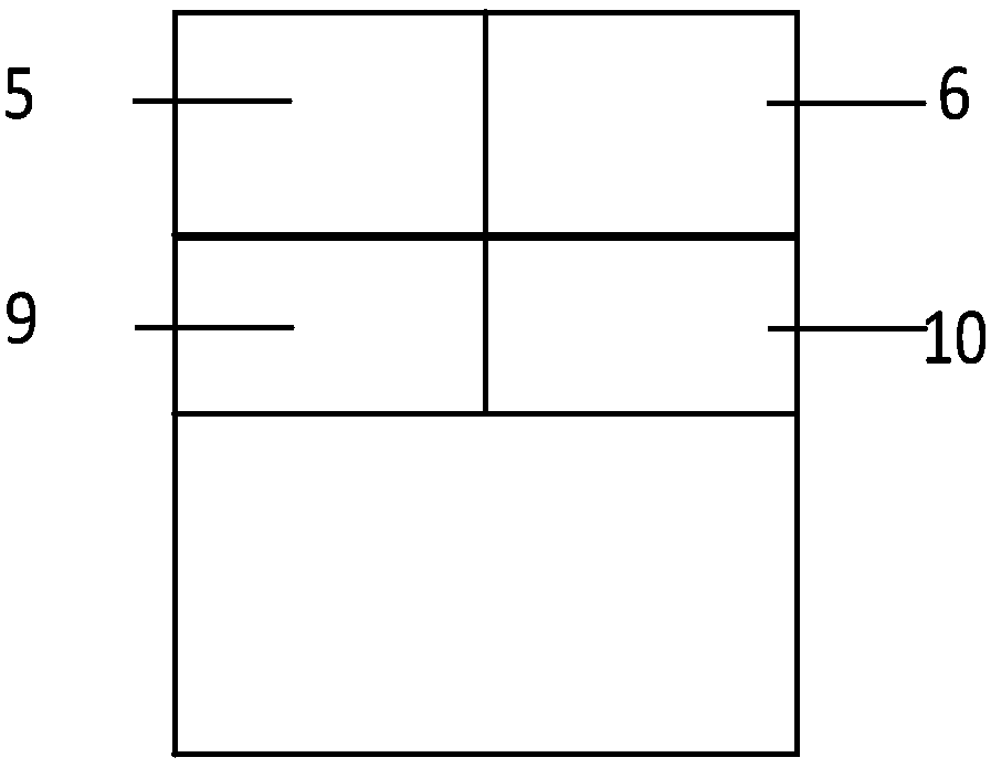
[0044] Implant N pillars and P pillars on the wide bandgap semiconductor material substrate at the edge of the base region, and arrange them alternately to form super junction (Super Junction) drift regions 5 and 6;

[0045] a source region 3 located on the surface of the base region;

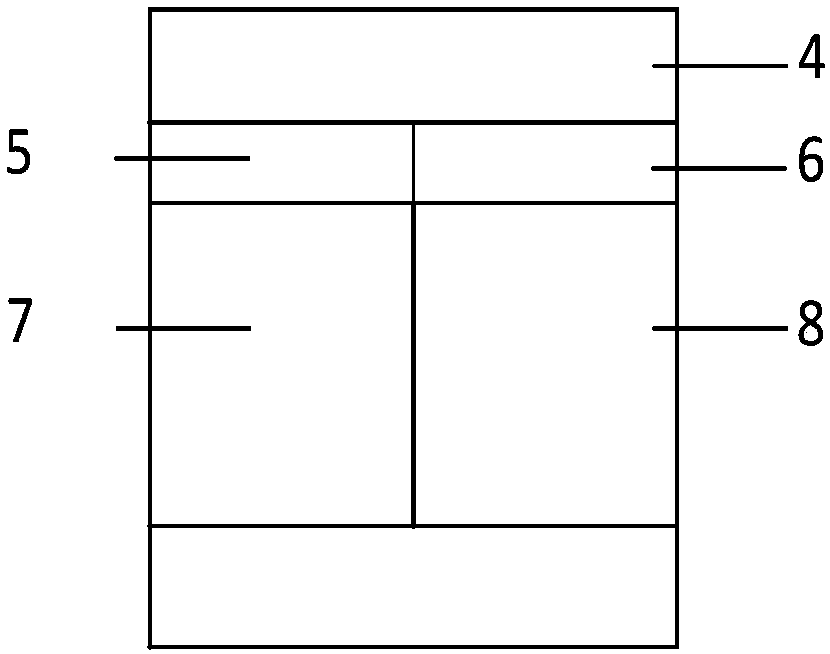
[0046] Drain region 4 located on the surface of super junction drift regions 5 and 6;

[0047] Below the super junction drift region at the drain end are vertical auxilia...


PUM


Abstract

The invention discloses a transverse and longitudinal electric field simultaneously optimized wide-bandgap semiconductor transverse superjunction double-diffused transistor. According to the structureof the transistor, a substrate-assisted depletion buried layer is disposed below the drift region of a drain terminal, and a substrate buried layer with charge compensation under the drift region isarranged near the substrate region of the substrate-assisted depletion buried layer; the substrate-assisted depletion buried layer can extend the longitudinal space charge area of the transverse super-junction double-diffused metal oxide semiconductor field-effect transistor, and the buried layer can modulate a horizontal electric field on the surface of the field-effect transistor and a longitudinal electric field inside the field-effect transistor by using an electric field modulation effect; the charge compensation substrate buried layer can eliminate the problem of substrate assisted depletion of a super-junction; new electric field peaks are introduced into the horizontal electric field on the surface of the field-effect transistor and the longitudinal electric field inside the transverse superjunction double-diffused metal oxide semiconductor field-effect transistor, so that the horizontal electric field on the surface and the longitudinal electric field inside the field-effect transistor electric field can be simultaneously optimized, and therefore, the breakdown voltage of the device can be greatly improved.

Description

technical field [0001] The invention relates to the technical field of semiconductor power devices, in particular to a lateral superjunction double-diffusion transistor. Background technique [0002] Lateral Double-diffused MOSFET (LDMOS) has the advantages of easy integration, good thermal stability, good frequency stability, low power consumption, multi-subconduction, small power drive, and switching speed Advanced advantages are at the heart of smart power circuits and high-voltage devices. However, due to the limitations of the first two generations of semiconductor materials represented by Si and GaAs, the third generation of wide-bandgap semiconductor materials has developed rapidly because of its excellent performance. Wide bandgap semiconductor materials have the characteristics of large bandgap width, high electron drift saturation velocity, small dielectric constant, and good electrical conductivity. Their superior properties and potential huge prospects in the fi...

Claims


Application Information

Patent Timeline
Patent Type & Authority Applications(China)
IPC IPC(8): H01L29/78H01L29/06
Inventor 段宝兴董自明杨银堂
Owner XIDIAN UNIV
Why Eureka
Try Eureka