Element semiconductor lateral super-junction double-diffused transistor with function of optimizing lateral and longitudinal electric fields synchronously

A semiconductor, horizontal and vertical technology, applied in the direction of semiconductor devices, electrical components, circuits, etc., can solve the problems of substrate-assisted depletion, limited optimization effect of lateral electric field, uneven distribution of surface electric field, etc.

Inactive Publication Date: 2018-03-06
XIDIAN UNIV
View PDF2 Cites 0 Cited by
  • Summary
  • Abstract
  • Description
  • Claims
  • Application Information

AI Technical Summary

Problems solved by technology

However, there are three problems in the super junction applied to LDMOS: 1) The P-type substrate of N-channel LDMOS assists in depleting the N-type region of the superjunction, which brings about the problem of substrate-assisted depletion (SAD) ; 2) Traditional SJ-LDMOS only forms electric field modulation between the N region and P region of the super junction, but there is no electric field modula...

Method used


Image

  • Element semiconductor lateral super-junction double-diffused transistor with function of optimizing lateral and longitudinal electric fields synchronously
  • Element semiconductor lateral super-junction double-diffused transistor with function of optimizing lateral and longitudinal electric fields synchronously
  • Element semiconductor lateral super-junction double-diffused transistor with function of optimizing lateral and longitudinal electric fields synchronously

Examples


Embodiment Construction

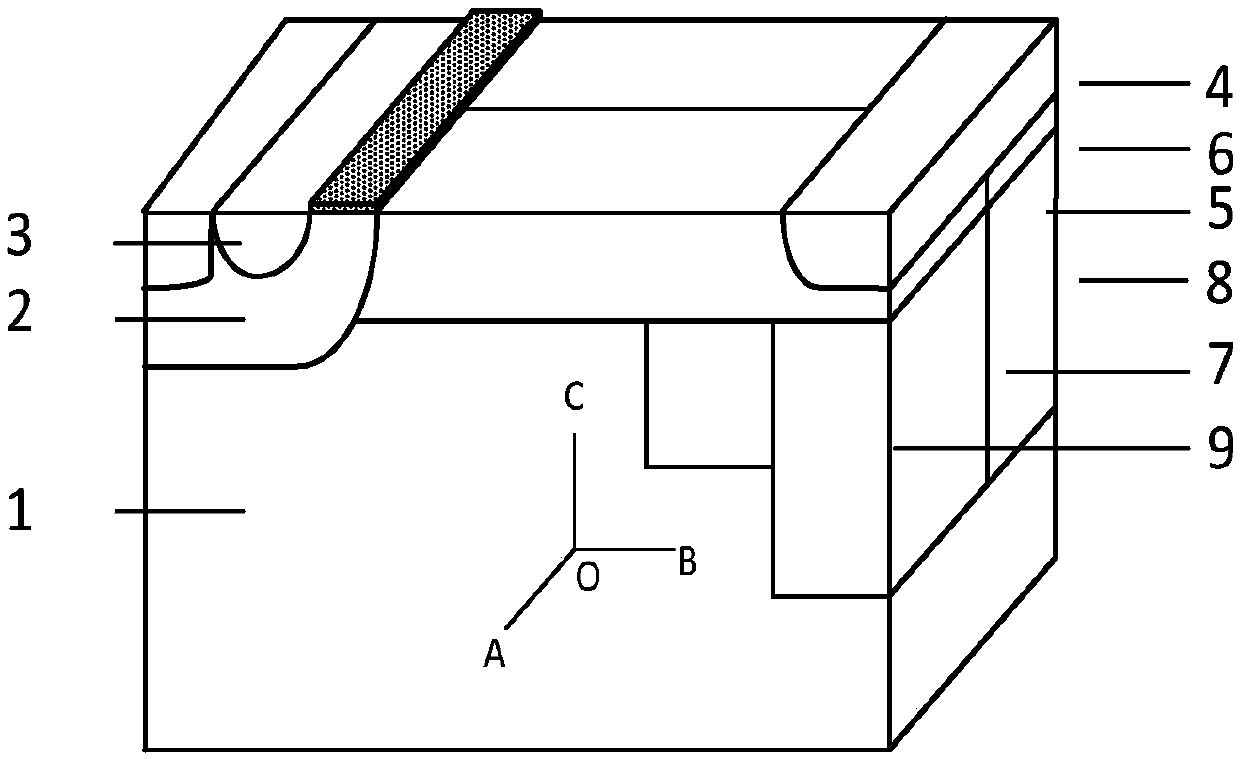
[0040] Such as figure 1 , figure 2 with image 3 Shown is a horizontal superjunction double-diffused transistor with horizontal and vertical electric fields while optimizing the elemental semiconductor:

[0041] Elemental semiconductor material substrate 1, the doping concentration is the concentration of general elemental semiconductor single crystal material, the typical value is 1×10 13 cm -3 ~1×10 15 cm -3 ;

[0042] a base region 2 located on the surface of the elemental semiconductor substrate;

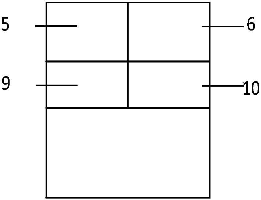
[0043] Implant N columns and P columns on the elemental semiconductor substrate at the edge of the base region, and arrange them alternately to form superjunction (SuperJunction) drift regions 5 and 6;

[0044] a source region 3 located on the surface of the base region;

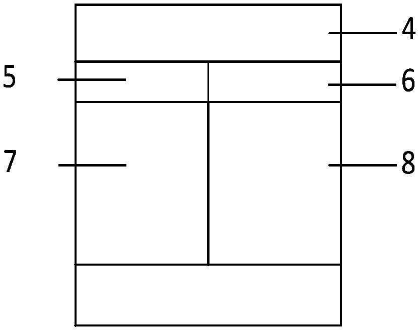
[0045] The drain region 4 located on the surface of the super junction drift region;

[0046] Below the drift region at the drain end are vertical auxiliary depletion substrate buried layers 7 and 8; ...


PUM

PropertyMeasurementUnit
Thicknessaaaaaaaaaa
Thicknessaaaaaaaaaa

Abstract

The invention discloses an element semiconductor lateral super-junction double-diffused transistor with a function of optimizing lateral and longitudinal electric fields synchronously. According to the structure, a substrate-assisted depletion buried layer is arranged below a drifting region at the drain end; and meanwhile, a substrate buried layer with a charge compensation function is arranged in a substrate region, close to the substrate-assisted depletion buried layer, below the drifting region. By virtue of the setting of the substrate-assisted depletion buried layer, a longitudinal spacecharge region of a lateral super-junction double-diffused metal oxide semiconductor field effect transistor can be expanded; by virtue of the buried layer, a surface lateral electric field and an in-vivo longitudinal electric field can be modulated through an electric field modulation effect; by virtue of the setting of the substrate buried layer with the charge compensation function, the problemof substrate-assisted depletion existing the super junction can be eliminated; and a new electric field peak is introduced to the surface lateral electric field and the in-vivo longitudinal electricfield of the lateral super-junction double-diffused metal oxide semiconductor field effect transistor separately, so that the surface lateral electric field and the in-vivo longitudinal electric fieldcan be optimized synchronously, thereby greatly improving the breakdown voltage of a device.

Description

technical field [0001] The invention relates to the technical field of semiconductor power devices, in particular to a lateral superjunction double-diffusion transistor. Background technique [0002] One of the most critical technologies for realizing power integrated circuit PIC (power integrated circuit) is that LDMOS (lateral double-diffused MOSFET) must have low on-resistance to reduce the power loss of PIC integrated circuit, while MOS devices are off-state. The 2.5th power relationship between the breakdown voltage and the on-state on-resistance limits the high-power application range of MOS devices. The superjunction structure alleviates this contradiction to the 1.33th power. Therefore, the superjunction technology is applied to LDMOS to form SJ- LDMOS is an effective way to realize ultra-low power consumption PIC. However, there are three problems in the super junction applied to LDMOS: 1) The P-type substrate of N-channel LDMOS assists in depleting the N-type regi...

Claims


Application Information

Patent Timeline
IPC IPC(8): H01L29/06H01L29/78
CPCH01L29/0623H01L29/0634H01L29/7816
Inventor 段宝兴董自明杨银堂
Owner XIDIAN UNIV
Why Eureka
Try Eureka