HEMT and method for adjusting electron concentration of HEMT

An electrode and electrode arrangement technology, applied in circuits, electrical components, semiconductor devices, etc., can solve problems such as damage to HEMT and heat loss

Inactive Publication Date: 2018-03-06
ROBERT BOSCH GMBH
View PDF6 Cites 0 Cited by
  • Summary
  • Abstract
  • Description
  • Claims
  • Application Information

AI Technical Summary

Problems solved by technology

[0003] The disadvantage here is that the discharge generates heat which causes losses and can destroy the HEMT

Method used


Image

  • HEMT and method for adjusting electron concentration of HEMT
  • HEMT and method for adjusting electron concentration of HEMT
  • HEMT and method for adjusting electron concentration of HEMT

Examples


Embodiment Construction

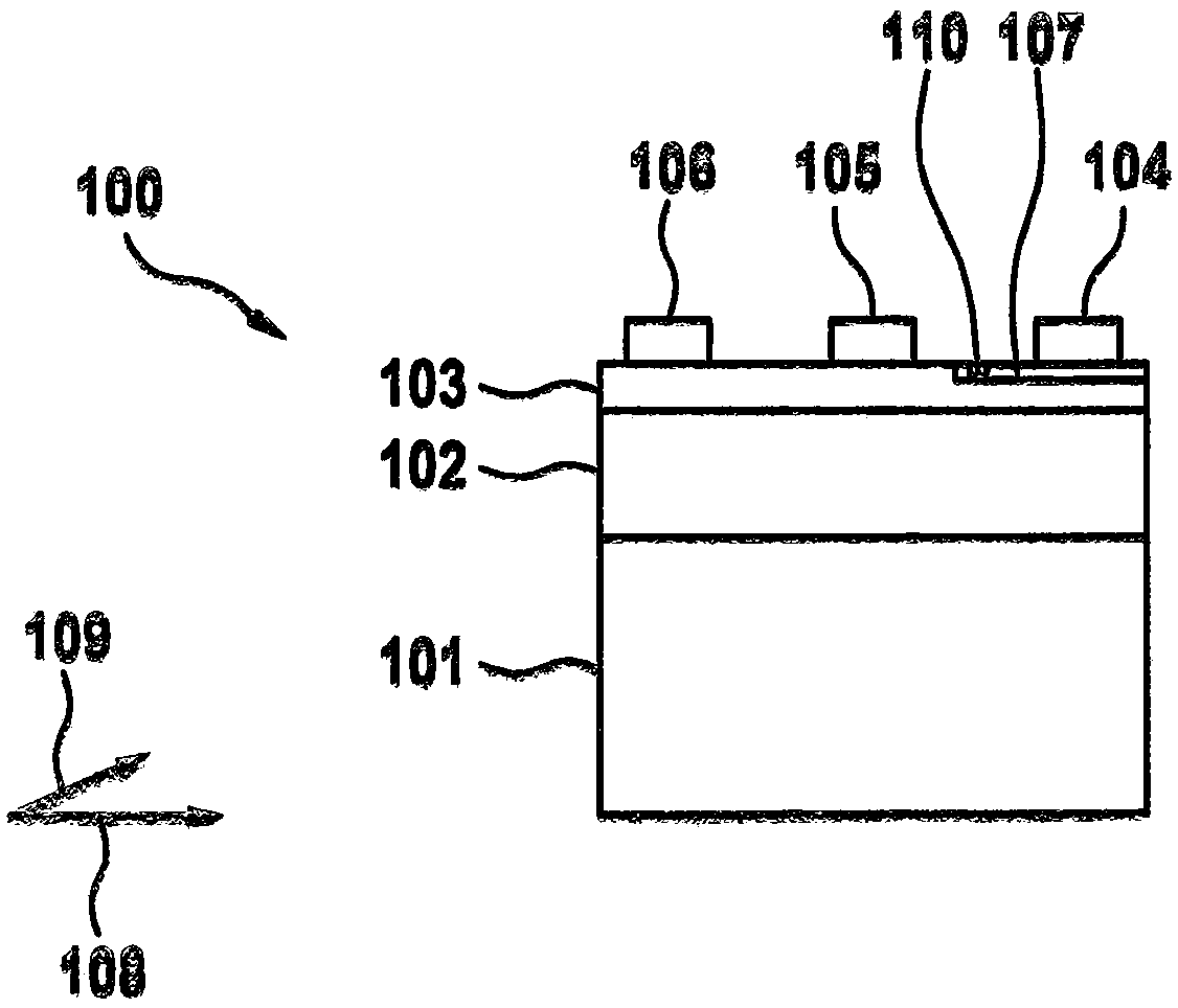
[0030] figure 1 A side view of a transistor 100 with high electron mobility is shown. The HEMT 100 includes a semiconductor substrate 101 , a first layer 102 and a second layer 103 . The first layer 102 is arranged on the semiconductor substrate 101 and the second layer 103 is arranged on the first layer 102 . The first layer 102 is also called a buffer layer, and the second layer 103 is also called a barrier layer. The buffer layer and the barrier layer each have a III-V semiconductor material and constitute a heterostructure of the HEMT 100 . Arranged on the second layer 103 are: a first electrode 104 , a second electrode 105 and a third electrode 106 . The first electrode 104 represents, for example, the drain connection of the HEMT 100 , the second electrode 105 represents, for example, the gate connection of the HEMT 100 and the third electrode 106 represents, for example, the source connection of the HEMT 100 . The first electrode 104 has a first side and a second si...


PUM


Abstract

The invention relates to a HEMT and a method for adjusting the electron concentration of a HEMT. The HEMT herein comprises: a semiconductor substrate having a first semiconductor substrate side and asecond semiconductor substrate side, the first semiconductor substrate side facing the second semiconductor substrate side; a first layer having a first side and a second side, the first side facing the second side, the first side of the first layer being disposed on the second semiconductor substrate side; a second layer having a first side and a second side, wherein a first side faces the secondside, the first side being disposed on the second side of the first layer; the first layer and the second layer forming a heterostructure, wherein the first layer and the second layer each comprisesa III-V semiconductor material; a first electrode having a first side and a second side, the first side of the first electrode facing the second side of the first electrode, the first side of the first electrode being disposed on the second side of the second layer, the first electrode having a length and a width; and a second electrode disposed on the second side of the second layer; at least onedrift region having a first direction perpendicular to the length of the first electrode and having a second direction parallel to the length of the first electrode, the first direction and the second direction being arranged perpendicular to each other, the drift region extending between the first electrode and the second electrode within the heterostructure which is characterized by having implanted regions.

Description

technical field [0001] The invention relates to a transistor with high electron mobility, a so-called HEMT and a method for adjusting the electron concentration of a HEMT. Background technique [0002] HEMTs have high output capacitance. In this case, the energy stored by means of the output capacitor is released during a hard or fast switching process of the HEMT. The key is mainly the switching frequency of several hundred kHz. [0003] The disadvantage here is that the discharge generates heat which causes losses and can destroy the HEMT. [0004] The object of the present invention is to provide a HEMT with low overall losses. Contents of the invention [0005] A transistor with high electron mobility (hereinafter referred to as HEMT) includes a semiconductor substrate having a first semiconductor substrate side and a second semiconductor substrate side, wherein the first semiconductor substrate side is connected to the second semiconductor substrate side The subst...

Claims


Application Information

Patent Timeline
Patent Type & Authority Applications(China)
IPC IPC(8): H01L29/778H01L29/06H01L29/36H01L21/335
CPCH01L29/0684H01L29/36H01L29/66462H01L29/778H01L29/0649H01L29/0653H01L29/2003H01L29/32H01L29/7786
Inventor S·基和安S·尧斯S·诺尔
Owner ROBERT BOSCH GMBH
Why Eureka
Try Eureka